Non-volatile memory device and method for fabricating the same

Pending Publication Date: 2022-08-25
UNITED MICROELECTRONICS CORP
View PDF3 Cites 0 Cited by
  • Summary
  • Abstract
  • Description
  • Claims
  • Application Information

AI Technical Summary

Benefits of technology

The patent describes a method to improve the performance of a non-volatile memory device called NVM. By making a modification to the recess where the memory cells are located, the cross-sectional area of the source region of each cell is increased, which leads to increased conduction current and reduced resistance. This modification also reduces the impact of the source loading effect, which helps to stabilize each memory cell. Additionally, the doping concentration of the modification can be increased to further reduce resistance and improve performance.

Problems solved by technology

When the source load of the memory cell string is changed (for example, when a read voltage is applied to these memory cells), the output (for example, read current) of each memory cell may be inconsistent with each other, due to the source loading effect, thereby the stability and reliability of the (reading) signal can be reduced, and the performance of these memory cells can be thus deteriorated (for example, causing the read failure of these memory cells).

Method used


Image

  • Non-volatile memory device and method for fabricating the same
  • Non-volatile memory device and method for fabricating the same
  • Non-volatile memory device and method for fabricating the same

Examples


Embodiment Construction

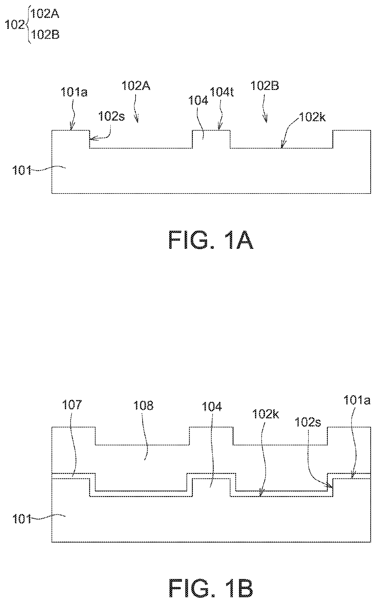
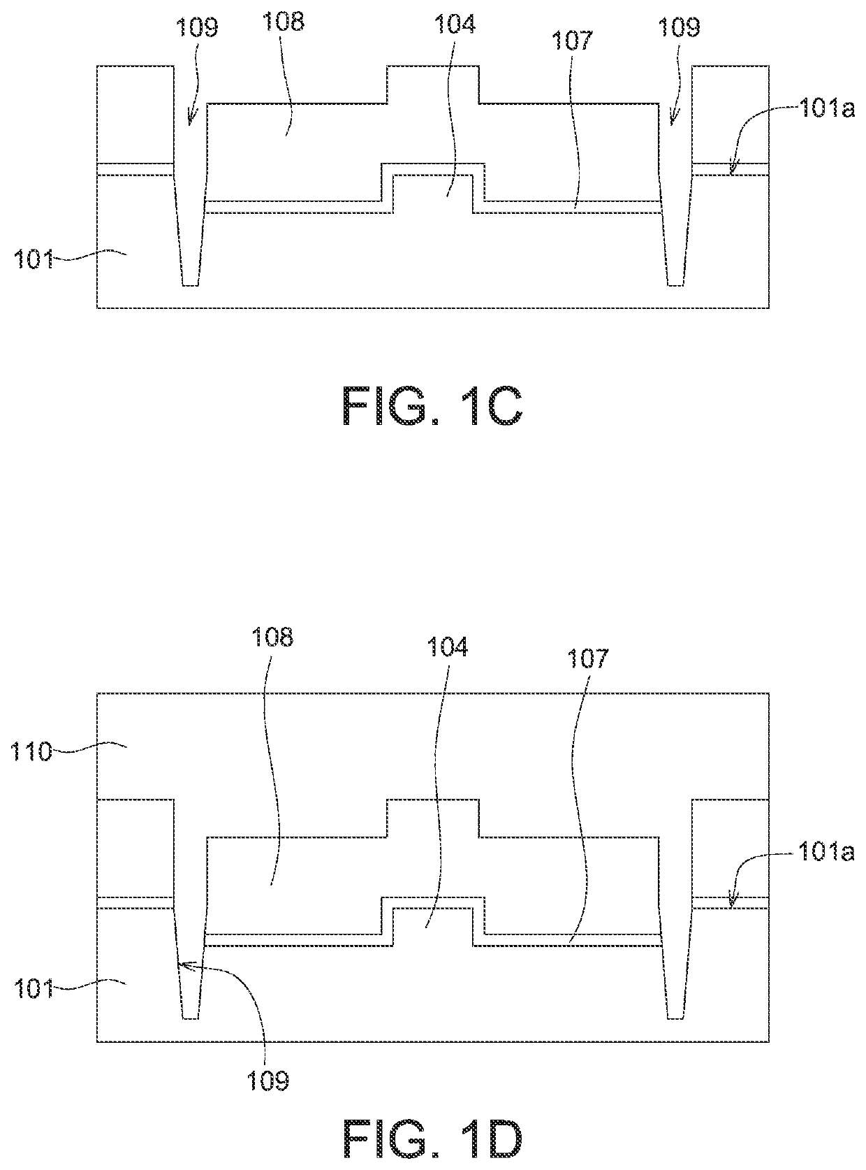
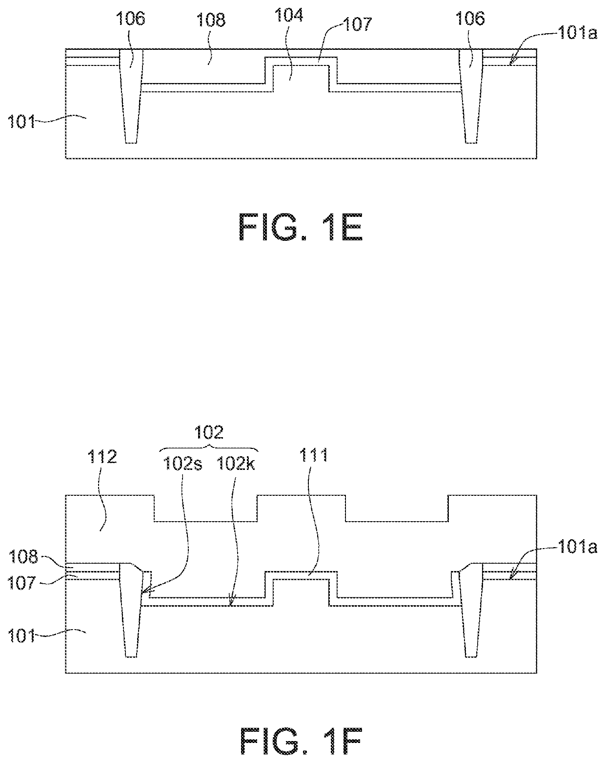
[0014]The embodiments as illustrated below provide an NVM device and the method for fabricating the same to reduce the negative impact of the source loading effect on the output stability of the memory cells. The present disclosure will now be described more specifically with reference to the following embodiments illustrating the structure and arrangements thereof.

[0015]It is to be noted that the following descriptions of preferred embodiments of this disclosure are presented herein for purpose of illustration and description only. It is not intended to be exhaustive or to be limited to the precise form disclosed. Also, it is important to point out that there may be other features, elements, steps, and parameters for implementing the embodiments of the present disclosure which are not specifically illustrated. Thus, the descriptions and the drawings are to be regard as an illustrative sense rather than a restrictive sense. Various modifications and similar arrangements may be provi...


PUM


Abstract

An NVM device includes a semiconductor substrate, a first floating gate, a first control gate, a first drain region, and a common source region. The semiconductor substrate has a recess extending downward from the substrate surface. The first floating gate is disposed in the recess, has a base and a side wall connecting to the base. The first control gate is disposed on and adjacent to the first floating gate. The first drain region is disposed in the semiconductor substrate in the recess. The common source region is formed in the semiconductor substrate in the recess, is adjacent to the first floating gate, and includes a main body and an extension part. The main body is disposed below a bottom surface of the recess and adjacent to the base. The extension part extends upward from the bottom surface beyond the base to be adjacent to the side wall.

Description

[0001]This application claims the benefit of People's Republic of China application Serial No. 202110212028.1 filed at Feb. 25, 2021, the subject matter of which is incorporated herein by reference.BACKGROUNDTechnical Field[0002]The disclosure relates to a memory device and the method for fabricating the same, and more particularly to a non-volatile memory (NVM) device and the method for fabricating the same.Description of Background[0003]An NVM device, such as a floating gate flash memory device, is able to continually store information even when the supply of electricity is removed from the device and has been widespreadly adopted by bulk solid state memory applications for portable music players, mobile phones, and digital cameras.[0004]A typical floating gate flash memory device includes a plurality of diffusion regions and isolation regions staggered along a first direction (for example, the x-axis direction) in the substrate; and further includes a plurality of gate structures...

Claims


Application Information

Patent Timeline
IPC IPC(8): H01L29/423H01L27/11521H01L29/51H01L29/78H01L29/788H01L21/265H01L21/28H01L29/66
CPCH01L29/42336H01L27/11521H01L29/42328H01L29/513H01L29/517H01L29/518H01L29/7833H01L29/7883H01L21/26513H01L29/40114H01L29/66492H01L29/66825H01L29/0847H01L29/788H10B41/35H01L29/40117H01L29/42344H01L29/792H10B41/30H10B43/30
Inventor YEH, YU-JENCHEN, CHIH-JUNG
Owner UNITED MICROELECTRONICS CORP
Why Eureka
Try Eureka