Semiconductor memory

Inactive Publication Date: 2006-11-16
SHARP KK
View PDF4 Cites 1 Cited by
  • Summary
  • Abstract
  • Description
  • Claims
  • Application Information

AI Technical Summary

Benefits of technology

[0007] The present invention has as an object to provide a semiconductor memory that can realize miniaturization and reduce resistance of a source diffusion layer.
[0009] As the foregoing describes, by (i) making the distance between (a) the interface between the upper-wall layer and the silicide and (b) the interface between the lower-wall layer and the silicide 1000 Å or shorter and (ii) making the depressed portion (trench) of the source diffusion layer shallow, the proportion of the side-wall layer in the source diffusion layer can be reduced. This makes it possible to shorten the path of the source diffusion layer, and therefore the resistance thereof can be reduced. Further, because the resistance is reduced by forming the silicide, it is not necessary to reduce the resistance at the time of forming the source diffusion layer by impurity implantation. This makes it possible to perform the implantation with less energy and less dosage. Therefore, the source diffusion layer can be prevented from expanding in the width direction (length in the direction orthogonal to the direction of extension), and miniaturization of the semiconductor memory can be realized. Further, in forming the silicide, the metal film (e.g., cobalt film) can be deposited with good coverage. Therefore, (i) an increase in resistance and (ii) wire breakage, both of which may occur if the silicide is formed improperly, can be prevented. Further, because no isolation layer is formed and the source diffusion layer is continuously formed, less implantation energy (than that in the case where the isolation layer is provided) is required for the impurity implantation performed to form the source diffusion layer. This makes it possible to miniaturize the source diffusion layer. As a result, (i) miniaturization of the semiconductor memory and (ii) reduction in the resistance of the source diffusion layer can be realized.

Problems solved by technology

The trench isolation, however, has a problem that a resistance of a source diffusion layer is increased when the source diffusion layer is formed by implantation using self-align source etching that employs anisotropic dry etching.
Therefore, it has been difficult to form a low-resistance source diffusion layer wiring on the side wall by ion-implantation.
However, in order to form the source diffusion layer in such a deep portion, high energy is required for ion-implantation of impurity.
This makes it difficult to shorten the width of the gate line by taking advantage of a short channel effect.
Thus, the semiconductor memory cannot be miniaturized.

Method used


Image

  • Semiconductor memory
  • Semiconductor memory
  • Semiconductor memory

Examples


Embodiment Construction

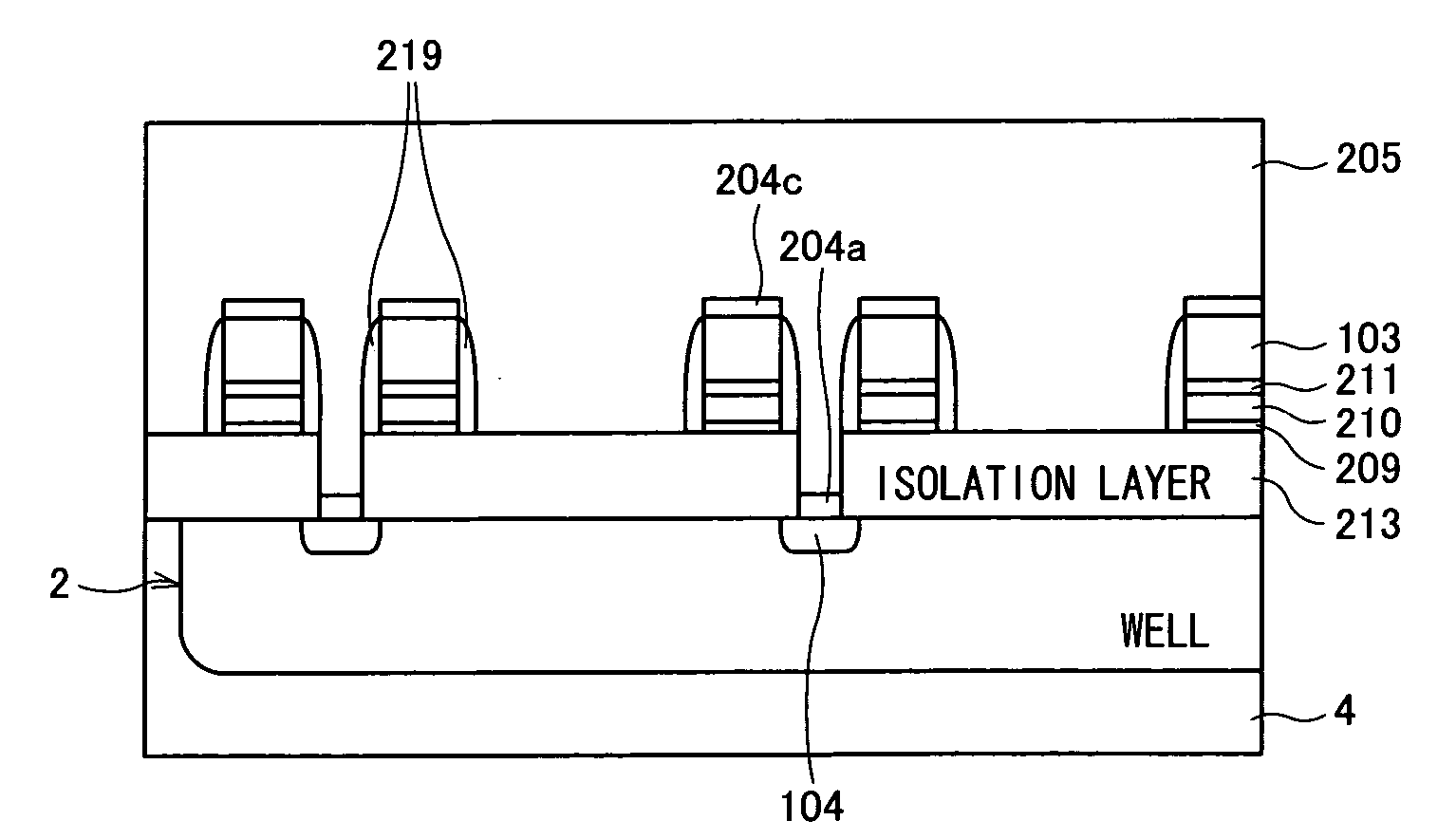
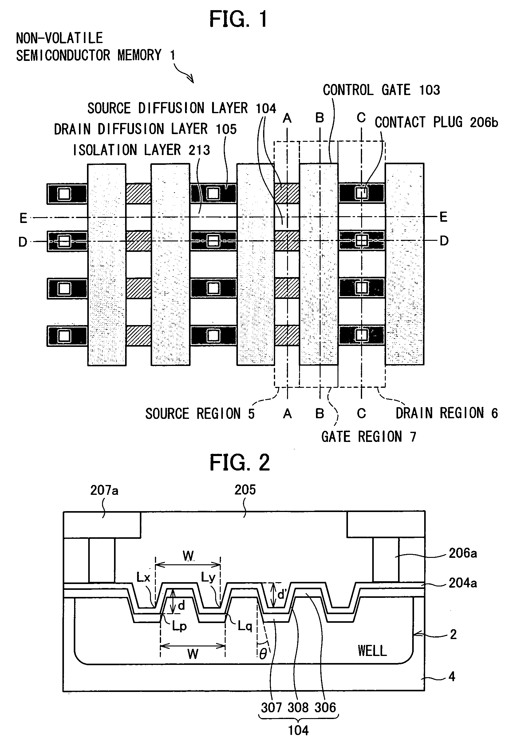
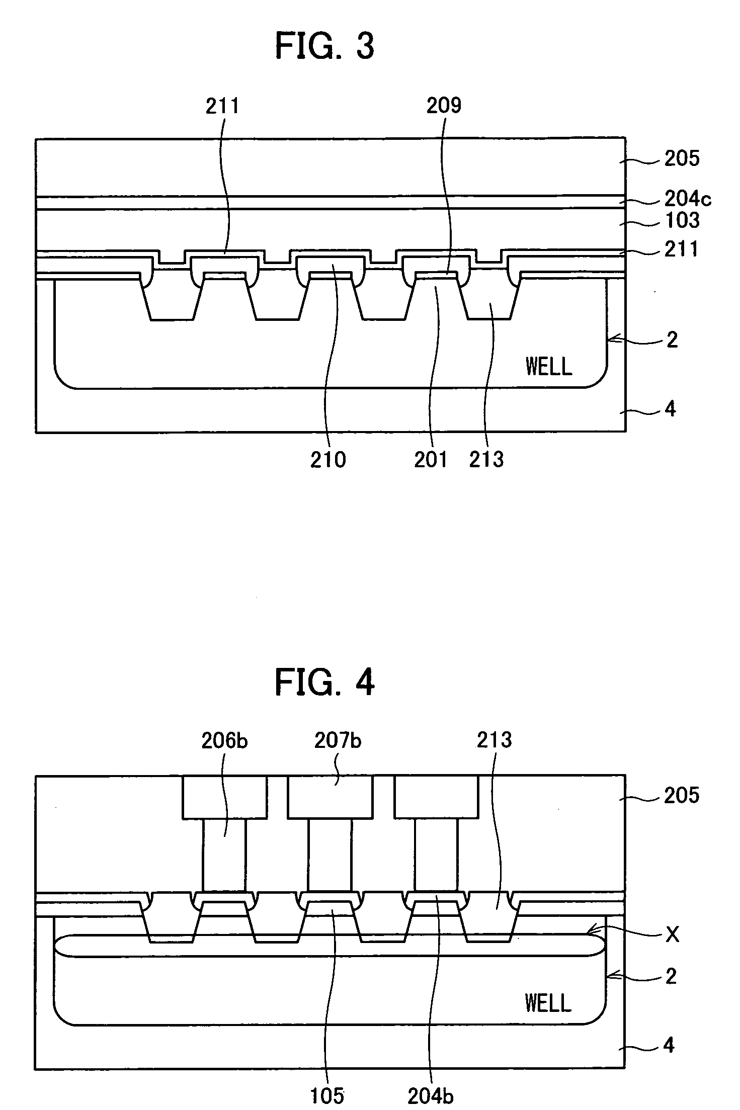
[0020] The following describes an embodiment of the present invention, with reference to FIGS. 1 to 9.

[0021]FIG. 1 is a perspective plane diagram illustrating a non-volatile semiconductor memory of the present embodiment. FIGS. 2 to 6 are cross sectional diagrams illustrating the non-volatile semiconductor memory.

[0022] As illustrated in FIGS. 1 to 6, the non-volatile semiconductor memory 1 of the present invention is provided with: a P-type well 2 formed on a substrate 4; a control gate 103; an N-type source diffusion layer 104; an N-type drain diffusion layer 105; a floating gate 210; an isolation layer 213; a silicide 204 (204a to 204c); an interlayer insulating film 205; a contact plug 206 (206a, 206b); and a metal wiring 207 (207a, 207b).

[0023] The non-volatile semiconductor memory 1 is arranged so that a source region 5, a drain region 6, and a gate region 7 are defined as illustrated in FIG. 1, as viewed from the top. Specifically, the source region 5 and the drain region ...


PUM


Abstract

In the non-volatile semiconductor memory in which an N-type source diffusion layer and an N-type drain diffusion layer are formed on a P-type well formed on a substrate: the source diffusion layer has a protrusion portion and a depressed portion on a cross section taken along a plane that includes (a) a straight line extending along a direction of extension of the source diffusion layer and (b) a normal line of the semiconductor substrate, and the source diffusion layer is formed of a series of (a) an upper-wall layer constituting the protrusion portion, (b) a lower-wall layer constituting the depressed portion, and (c) a side-wall layer between the upper-wall layer and the lower-wall layer; a silicide is formed to cover the upper-wall layer, the lower-wall layer, and the side-wall layer, and an insulating layer is formed to cover the silicide; and a distance d between (a) an interface between the insulating layer and the silicide formed on the upper-wall layer and (b) an interface between the insulating layer and the silicide formed on the lower-wall layer is 1000 Å or shorter. This structure allows (i) miniaturization of the non-volatile semiconductor memory and (ii) reduction in a resistance of the source diffusion layer of the non-volatile semiconductor memory.

Description

[0001] This Nonprovisional application claims priority under 35 U.S.C. § 119(a) on Patent Application No. 137541 / 2005 filed in Japan on May 10, 2005, the entire contents of which are hereby incorporated by reference. FIELD OF THE INVENTION [0002] The present invention relates to a semiconductor memory (e.g., non-volatile memory), and in particular, to (i) a structure of a source diffusion layer and (ii) a fabrication method thereof. BACKGROUND OF THE INVENTION [0003] For isolation of a structure in a non-volatile semiconductor memory (e.g., flash memory), a trench isolation is commonly employed. The trench isolation, however, has a problem that a resistance of a source diffusion layer is increased when the source diffusion layer is formed by implantation using self-align source etching that employs anisotropic dry etching. Moreover, with the trench isolation, the side wall of the trench is inclined sharply at an angle close to 0°. Therefore, it has been difficult to form a low-resis...

Claims


Application Information

Patent Timeline
IPC IPC(8): H01L29/80H01L21/336H01L21/76H01L27/115H01L27/11521H01L29/788H01L29/792
CPCH01L27/11521H01L27/115H10B69/00H10B41/30H01L21/32051H10B41/10
Inventor HIRONAKA, KATSUYASATO, SHINICHI
Owner SHARP KK
Why Eureka
Try Eureka