Integration method of vertical nanowire device of air side wall structure

An air-side, nanowire technology, applied in the manufacture of electrical components, semiconductor devices, semiconductor/solid-state devices, etc., can solve the problems of difficult to control the channel cross-sectional morphology, degradation of device characteristics consistency, affecting the high-frequency characteristics of devices, etc. Achieve the effect of reducing penetration, reducing the degradation of on-state current, and improving frequency characteristics

Active Publication Date: 2016-10-26
PEKING UNIV
View PDF6 Cites 2 Cited by
  • Summary
  • Abstract
  • Description
  • Claims
  • Application Information

AI Technical Summary

Problems solved by technology

[0005] With the shrinking of the size of vertical nanowire devices, the proportion of source-drain parasitic resistance and parasitic capacitance in the total resistance increases sharply. Among the parasitic resistance, the source resistance has the greatest influence on the on-state current, while the parasitic capacitance of the drain is due to the dense The Le effect will be magnified several times, greatly affecting the high frequency characteristics of the device;
[0006] Forming a vertical channel with a smaller diameter and a large aspect ratio by etching poses a great challenge to the etching process, and the cross-sectional shape of the channel formed by etching is difficult to control, resulting in the degradation of the consistency of device characteristics. , channel damage caused by etching, causing further degradation of device performance;

Method used


Image

  • Integration method of vertical nanowire device of air side wall structure
  • Integration method of vertical nanowire device of air side wall structure
  • Integration method of vertical nanowire device of air side wall structure

Examples


Embodiment Construction

[0089] The present invention will be described in detail below in conjunction with the accompanying drawings and specific examples.

[0090] A vertical nanowire NMOSFET with an air sidewall structure on an SOI substrate can be realized according to the following steps:

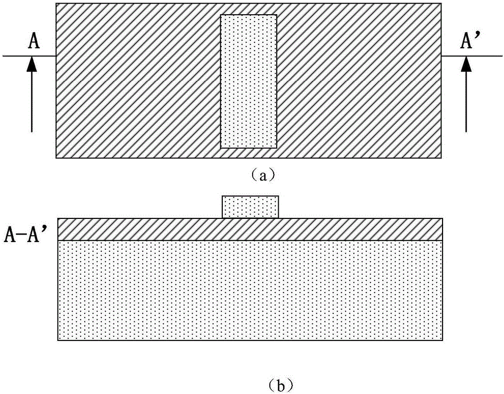
[0091] 1) On the (100) P-type lightly doped SOI substrate, use HNA solution to thin the top silicon film to 20nm, define the lower active region of the device by photolithography and RIE etching, and remove the glue, such as figure 1 shown;

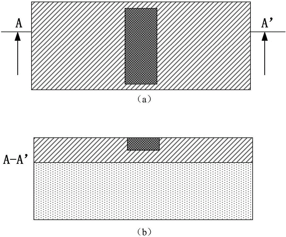
[0092] 2) Perform As + Implant doping to form the lower active region of the device (as the source end of the device), the implantation energy is 10KeV, and the implantation dose is 5E15cm -2 ;

[0093] 3) LPCVD SiO 2 40nm, the surface is planarized by chemical mechanical polishing, exposing the upper surface of the active region under heavy doping, forming STI, such as figure 2 shown;

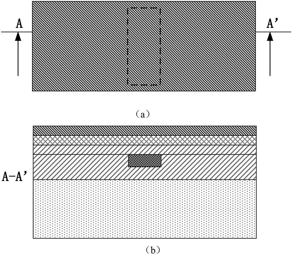
[0094] 4) Deposit 10nm SiO sequentially by ALD 2 (as the SDE mask layer 1, ...


PUM


Abstract

The invention provides an integration method of a vertical nanowire device of an air side wall structure. In the method, through hole etching and epitaxial channel material integration are combined, and an upper active area air side wall structure is manufactured. Compared to a traditional silicon dioxide or silicon nitride side wall structure, in the structure of the invention, a relative dielectric constant of air is 1 so that a stray capacitance between a grid electrode and an upper active area can be greatly reduced; the upper active area is taken as a drain terminal of the device, and a stray capacitance of the drain terminal is optimized so that a frequency characteristic of the device can be greatly improved. Simultaneously, a lower active extension area is heavily doped and is taken as a source terminal of the device so that a source terminal resistance can be reduced and degeneration of a device on state current is decreased. Light doping of one side of the channel in an upper active extension area is transited into heavy doping of one side of the upper active area so that penetration of a drain terminal electric field to a channel area can be reduced and simultaneously a low drain terminal resistance is maintained. The method is compatible with a traditional integration circuit manufacturing technology. The technology is simple and cost is low.

Description

technical field [0001] The invention belongs to the technical field of VLSI manufacturing and relates to an integration method of vertical nanowire devices with an air sidewall structure. Background technique [0002] When the semiconductor device enters the 22nm technology generation, the horizontal channel three-dimensional multi-gate device (Multi-gate MOSFET, MuGFET) represented by the fin field effect transistor (FinFET) has outstanding ability to suppress short channel effect, high integration density, Compatible with traditional CMOS technology and other advantages, it has become the mainstream of semiconductor devices. However, when moving towards a smaller size technology node, it is difficult to reduce the pitch of contact holes (limiting the increase in integration density), and gate etching on complex topography. [0003] Vertical trench gate devices have attracted much attention because of their advantages such as higher integration density, asymmetric source-d...

Claims


Application Information

Patent Timeline
IPC IPC(8): H01L21/336H01L29/06
CPCH01L29/0669H01L29/66545H01L29/66553H01L29/66666
Inventor 黎明陈珙杨远程黄如
Owner PEKING UNIV
Why Eureka
Try Eureka