Interconnection structure and manufacture method thereof

a technology of interconnection structure and manufacturing method, which is applied in the direction of semiconductor devices, semiconductor/solid-state device details, electrical apparatus, etc., can solve the problems of increasing the size of the die, preventing the state-of-the-art interconnection system from being allowed, and blocking some efficient channeling

Pending Publication Date: 2022-09-15
INVENTION & COLLABORATION LAB PTE LTD
View PDF0 Cites 6 Cited by
  • Summary
  • Abstract
  • Description
  • Claims
  • Application Information

AI Technical Summary

Problems solved by technology

By so far, the state-of-the-art interconnection system may not allow, for example, that the gate directly connect to M2 without bypassing the M1 structure.
As results, the necessary space between one M1 interconnection and the other M1 interconnection can increase the die size and in some cases the wiring connections may block some efficient channeling intention of using M2 directly to surpass M1 regions.
In addition, there is no method to form a self-alignment structure between Via1 to contact and at the same time both Via1 and contact are connected to their own interconnection systems, respectively.

Method used


Image

  • Interconnection structure and manufacture method thereof
  • Interconnection structure and manufacture method thereof
  • Interconnection structure and manufacture method thereof

Examples


embodiment 1

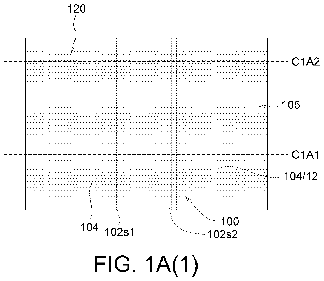
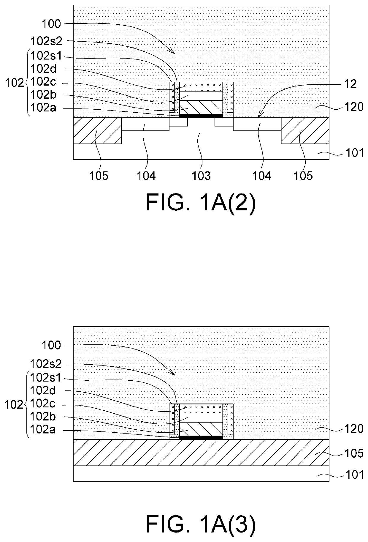
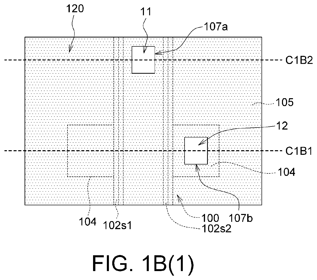
[0106]According to one embodiment of the present disclosure, the method for forming a device 10 having a transistor structure 100 includes steps as follows:

[0107]Step S11: forming a first dielectric layer over a first terminal of a device.

[0108]Step S12: forming a conductor pillar connected to the first terminal.[0109]Step S121: forming an open hole in the first dielectric layer to reveal a silicon region of the first terminal.[0110]Step S122: forming a first conductor pillar portion on the silicon region of the first terminal by a first selective epitaxy growth.[0111]Step S123: forming a first dielectric sub-layer over the first dielectric layer, wherein a top surface of the first dielectric sub-layer has a level substantially the same as that of the first conductor pillar portion (such as planarized by CMP process or etching process).[0112]Step S124: forming a second conductor pillar portion on the first conductor pillar by a second selective epitaxy growth.

[0113]Step S13: forming...

embodiment 2

[0145]According to one embodiment of the present disclosure, the method for forming a device 20 having a transistor structure 200 includes steps as follows:

[0146]Step S21: forming a first dielectric layer over a first terminal and a second terminal of a device.

[0147]Step S22: simultaneously forming a first silicon pillar passing through the first dielectric layer and connected to the first terminal and forming a second silicon pillar passing through the first dielectric layer and connected to the second terminal.[0148]Step S221: forming open holes in the first dielectric layer to reveal a silicon region of the first terminal and a silicon region of the second terminal.[0149]Step S222: simultaneously forming the first silicon pillar on the silicon region of the first terminal and forming the second silicon pillar on the silicon region of the second terminal by a selective epitaxy growth.

[0150]Step S23: forming a first conduction layer over the first dielectric sub-layer.

[0151]Referri...

embodiment 3

[0163]According to one embodiment of the present disclosure, the method for forming a device 30 having a transistor structure 200 includes steps as follows:

[0164]Step S31: forming a first dielectric layer over a first terminal and a second terminal of a device.

[0165]Step S32: simultaneously forming a first silicon pillar passing through the a first dielectric layer and connected to the first terminal and forming a second silicon pillar passing through the a first dielectric layer and connected to the second terminal.[0166]Step S321: forming open holes in the first dielectric layer to reveal a silicon region of the first terminal and a silicon region of the second terminal.[0167]Step S322: simultaneously forming the first silicon pillar on the silicon region of the first terminal and forming the second silicon pillar on the silicon region of the second terminal by a selective epitaxy growth.

[0168]Step S33: replacing the first silicon pillar by a first conductor pillar and replacing t...


PUM


Abstract

An interconnection structure includes a first dielectric layer, a first conduction layer, a conductor pillar, an upper dielectric layer and an upper conduction layer. The first dielectric layer is disposed over a first terminal of a device. The first conduction layer is disposed over the first dielectric layer. The conductor pillar is connected to the first terminal. The upper dielectric layer is disposed over the first conduction layer. The upper conduction layer is disposed over the upper dielectric layer. The conductor pillar connects to the upper conduction layer but disconnects from the first conduction layer.

Description

[0001]This application claims the benefit of U.S. provisional application Ser. No. 63 / 158,896, filed Mar. 10, 2021, the subject matter of which is incorporated herein by reference.BACKGROUND OF THE DISCLOSUREField of the Disclosure[0002]The disclosure relates in general to a semiconductor structure and the manufacture method thereof, and more particularly to an interconnection structure and the manufacture method thereof.Description of the Related Art[0003]A current Integrated-circuits chip has many transistors which are connected by a one-die interconnection system of using multiple interconnections, which has its first interconnection layer M1 to connect the gate-level (Gate) and the diffusion-level of the source-region and the drain-region (called generally as Diffusion) of the MOSFET device. When there is a need to increase a second interconnection layer M2 for facilitating signal transmission without enlarging the die size by only using M1, then a structure Via-1, which is comp...

Claims


Application Information

Patent Timeline
Patent Type & Authority Applications(United States)
IPC IPC(8): H01L23/522H01L21/768
CPCH01L23/5226H01L21/76885H01L23/53266H01L21/76897H01L21/28525H01L21/76805H01L23/485
Inventor LU, CHAO-CHUN
Owner INVENTION & COLLABORATION LAB PTE LTD
Why Eureka
Try Eureka