Eureka AIR delivers breakthrough ideas for toughest innovation challenges, trusted by R&D personnel around the world.

Electronic device and manufacturing method of the same

Pending Publication Date: 2022-10-27
RAYNERGY TEK INC +1
View PDF2 Cites 0 Cited by
  • Summary
  • Abstract
  • Description
  • Claims
  • Application Information

AI Technical Summary

Benefits of technology

The present invention provides an electronic device and a manufacturing method that includes a semiconductor layer with connecting channels formed by multiple laser processing with different powers. The connecting channels are formed between the lower electrodes and the upper electrodes of the electronic components, and a conductive material is configured in the connecting channels to electrically connect the upper electrodes. The manufacturing method includes steps of forming the lower electrodes and insulating material on the substrate, forming the semiconductor layer on the insulating material, and performing multiple laser processing on the semiconductor layer to form the connecting channels. The technical effect of the invention is to provide an electronic device with improved electrical connection between the upper electrodes of different electronic components.

Problems solved by technology

In view of global warming, climate change has become a common challenge in the international communities.
In order to improve the photoelectric conversion efficiency of electronic device, in addition to improving the materials of the electronic device, the improvement of the manufacturing process of the electronic device is also one of the important issues to maximize the effectiveness of the materials.
Due to the manufacturing process is a large-area manufacturing, it is easy to cause problems that are easily visible in mass production, and it is also easy to produce uneven manufacturing process defects.
For example, when the semiconductor layer material is deposited on a large area, the thickness of the semiconductor layer material in each area will inevitably be different, which will easily affect the subsequent laser ablation and series and parallel connections.
However, when the single-power laser is ablated on the semiconductor layer materials of different thicknesses, the problem of inconsistent laser ablation levels will occur.
Then, the connection channels among electronic components may not be conductive due to incomplete ablation, or the structure of the lower electrode is damaged due to excessive ablation, which in turn leads to problems such as a decrease in the electrical conductivity of the lower electrode itself.
In this regard, how to improve the influence of the uneven thickness of the semiconductor layer material on the subsequent laser ablation is a very important issue at present.

Method used


Image

  • Electronic device and manufacturing method of the same
  • Electronic device and manufacturing method of the same
  • Electronic device and manufacturing method of the same

Examples


Embodiment Construction

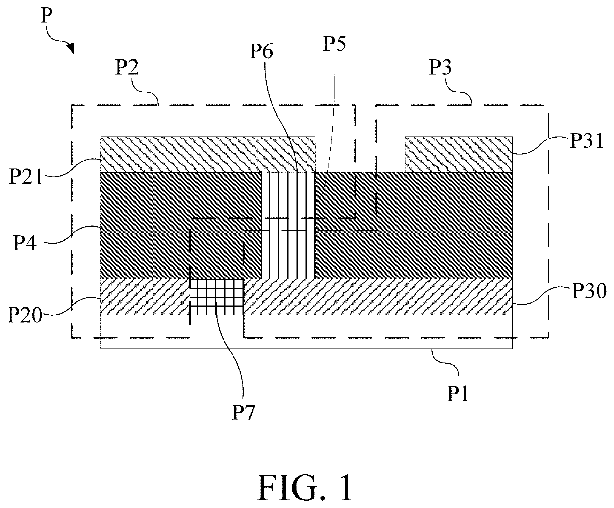
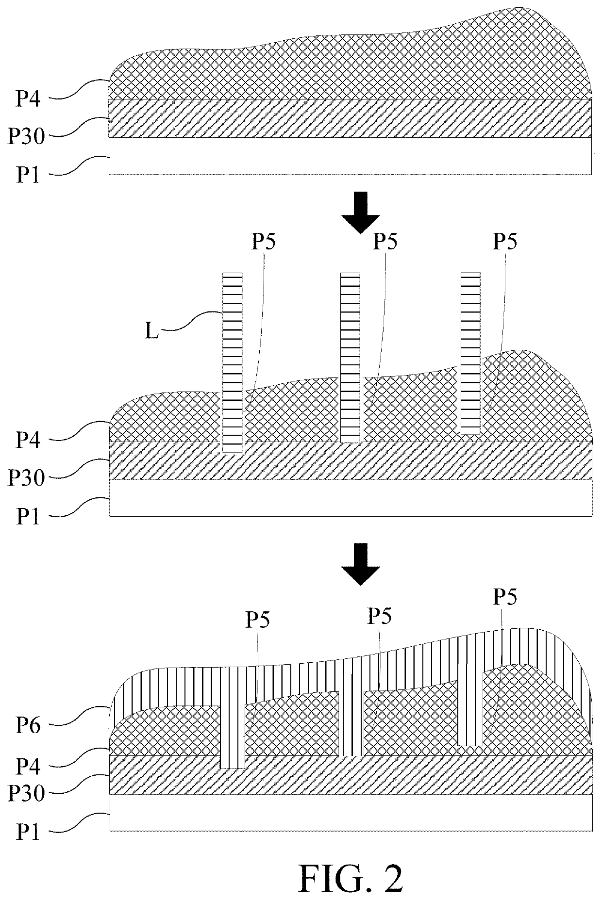
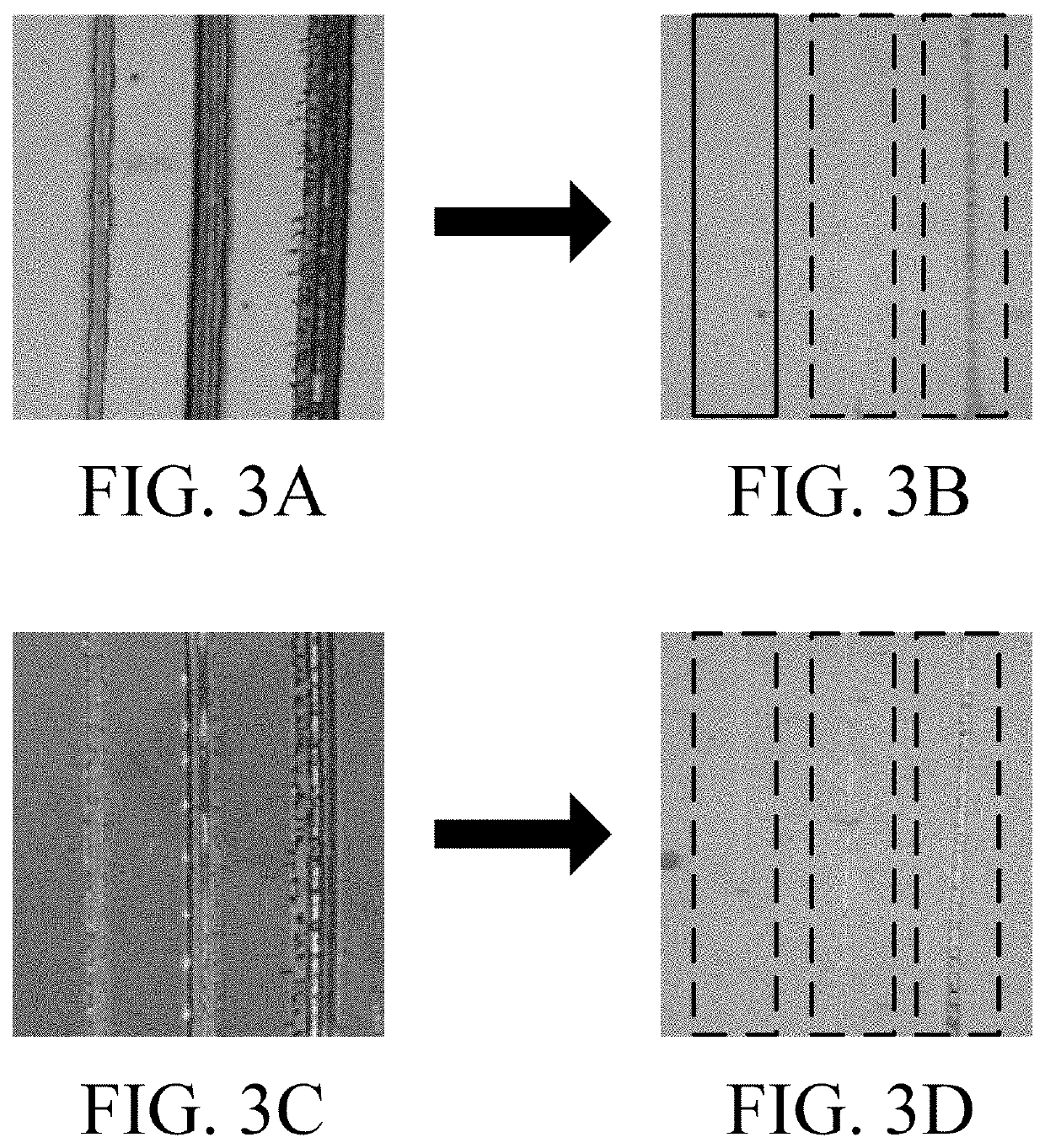
[0034]In order to make the advantages, spirit and features of the present invention easier and clearer, it will be detailed and discussed in the following with reference to the embodiments and the accompanying drawings. It is worth noting that the specific embodiments are merely representatives of the embodiments of the present invention, but it can be implemented in many different forms and is not limited to the embodiments described in this specification. Rather, these embodiments are provided so that this disclosure will be thorough and complete.

[0035]The terminology used in the various embodiments disclosed in the present invention is only for the purpose of describing specific embodiments, and is not intended to limit the various embodiments disclosed in the present invention. As used herein, singular forms also include plural forms unless the context clearly indicates otherwise. Unless otherwise defined, all terms (including technical and scientific terms) used in this specifi...


PUM


Abstract

An electronic device includes a substrate, a plurality of electronic components and a conductive material. The electronic components are arranged on the substrate, and the electronic components respectively include a lower electrode, a semiconductor layer and an upper electrode, and they are sequentially stacked on the substrate. The electronic components share the semiconductor layer, and the semiconductor layer forms a plurality of connecting channels through the semiconductor layer. The connecting channels are located between the upper electrode of the first electronic component in the electronic components and the lower electrode of the second electronic component in the electronic components. These connecting channels are processed by lasers of different powers. The conductive material is arranged in the connecting channel so that the upper electrode of the first electronic component is electrically connected to the lower electrode of the second electronic component.

Description

[0001]The present application is based on, and claims priority from, Republic of China (Taiwan) application number TW110115126, filed on 2021 Apr. 27, the disclosure of which is hereby incorporated by reference herein in its entirety.BACKGROUND OF THE INVENTIONField of the invention[0002]The present invention relates to an electric device comprising a plurality of electronic components electrically connecting with each other, and a manufacturing method of the electric device.Description of the Prior Art[0003]In view of global warming, climate change has become a common challenge in the international communities. The Kyoto protocol proposed by the “United Nations Framework Convention on Climate Change (UNFCCC)” in 1997 which had entered into force in 2005 is aimed at reducing carbon dioxide emissions. In this regard, countries are focusing on the development of renewable energy to reduce the use of petrochemical fuels. As the sun provides far enough energy needs of people at present ...

Claims


Application Information

Patent Timeline
IPC IPC(8): H01L31/18H01L31/0392H01L31/0224
CPCH01L31/1804H01L31/0392H01L31/1852H01L31/022425H01L31/0463H01L31/0465
Inventor CHANG, YI-MINGLEE, CHUN-CHIEHKAO, JUI-CHIHTENG, NAI-WEI
Owner RAYNERGY TEK INC
Why Eureka
Eureka Blog
Learn More