Process for rounding an intersection between an HSG-SI grain and a polysilicon layer

a polysilicon layer and hsg-si technology, applied in the direction of capacitors, semiconductor devices, electrical equipment, etc., can solve the problems of inability to achieve appreciably larger capacitance electrodes than conventional polysilicon, and inability to achieve further improvement of capacitance using hsg-

Inactive Publication Date: 2000-01-11
UNITED MICROELECTRONICS CORP
View PDF8 Cites 10 Cited by
  • Summary
  • Abstract
  • Description
  • Claims
  • Application Information

AI Technical Summary

Problems solved by technology

Further reductions in capacitance would require more frequent refresh operations for the DRAM, which are undesirable because at least portions of the DRAM are unavailable for the reading and writing of information during refresh operations.
Substrate deposition temperatures of ten degrees higher or lower than 590.degree. C. produced an unacceptable surface texture, that is, these conditions produced an undesirably flat surface which did not provide appreciably larger capacitance electrodes than conventional polysilicon.
The use of HSG-Si within lower electrodes of DRAM capacitors has been successful in approximately doubling the capacitance of DRAM capacitors, but no further improvements in capacitance have been obtained using HSG-Si.
A difficulty that has been encountered in the implementation of capacitors incorporating HSG-Si is that excessive leakage currents have been observed for capacitors incorporating HSG-Si electrodes.
Because of the incidence of high leakage currents, it has been difficult to use very thin dielectric layers for the capacitor dielectric layers.

Method used


Image

  • Process for rounding an intersection between an HSG-SI grain and a polysilicon layer
  • Process for rounding an intersection between an HSG-SI grain and a polysilicon layer
  • Process for rounding an intersection between an HSG-SI grain and a polysilicon layer

Examples


Embodiment Construction

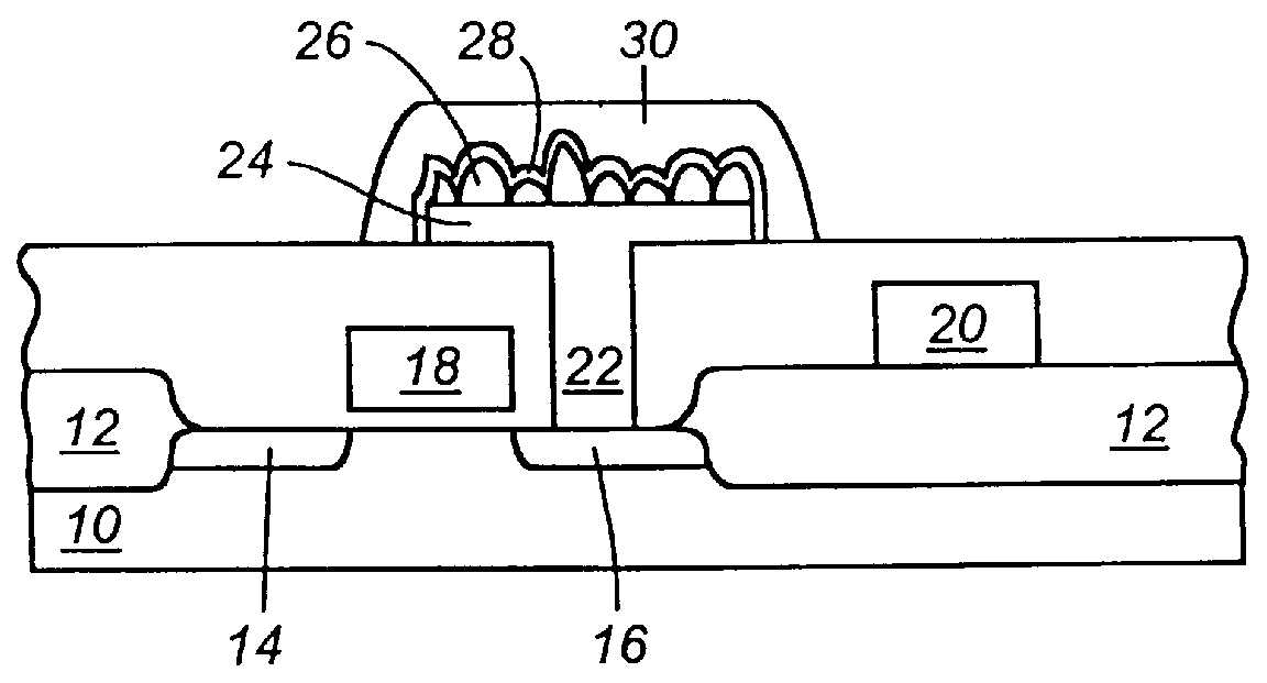
It is accordingly an object of this invention to provide a method of forming an HSG-Si layer in the process of making an electrode that is more compatible with the use of thin dielectric films on the HSG-Si electrode.

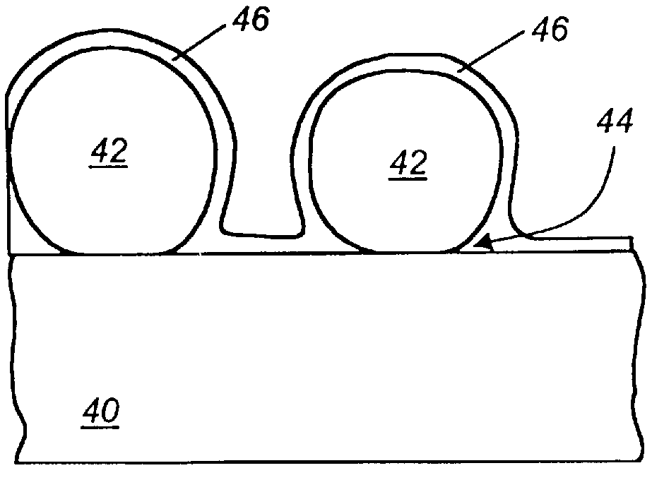
One aspect of the present invention forms a semiconductor device by providing a layer of polysilicon on or above a silicon substrate and then providing a layer of hemispherical-grained silicon on the layer of polysilicon. A layer of amorphous silicon is provided on the layer of hemispherical-grained silicon and on any exposed portions of the layer of polysilicon. A dielectric layer is formed over a surface of the layer of amorphous silicon.

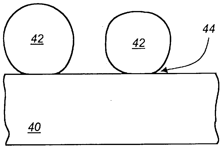
Another aspect of the present invention provides a method of making a semiconductor device comprising the steps of providing a deposition substrate on or above a silicon substrate and providing a layer of hemispherical-grained silicon on the deposition substrate. A layer of conductive material is provided on the layer of hemispherical...


PUM


Abstract

The capacitor of a DRAM cell is formed by depositing a layer of doped polysilicon, patterning the layer of doped polysilicon to define the extent of the capacitor's lower electrode and depositing a layer of hemispherical-grained silicon (HSG-Si) on the layer of doped polysilicon. A thin layer of amorphous silicon is then formed over the HSG-Si layer. This textured polysilicon structure forms the lower electrode of the DRAM capacitor. A dielectric layer is formed on the lower electrode, and an upper electrode is formed from a second layer of doped polysilicon. As-formed HSG-Si grains tend to form sharp intersections with the polysilicon layers on which they grow. When these HSG-Si grains are exposed to a thermal oxidation environment, poor quality oxides are formed at the sharp corners between the HSG-Si grains and the doped polysilicon layer. The poor quality oxides at the sharp corners between the HSG-Si grains and the doped polysilicon layer break down comparatively readily, and appears to cause leakage currents in capacitors having HSG-Si electrodes. By growing a thin amorphous silicon layer over the surface of the HSG-Si layer, the intersection between the HSG-Si grains and the layer of polysilicon is rounded. Subsequent growth of a thermal oxide, or the formation of other dielectric layers, provides a more reliable capacitor.

Description

1. Field of the InventionThe present invention relates to the formation of high capacitance structures in integrated circuit devices and, more particularly, to the formation of electrodes which incorporate at least one textured surface.2. Description of the Related ArtHistorically, increasing the density of integrated circuit devices has been accomplished in part by decreasing the size of structures such as wiring lines and transistor gates and by decreasing the separation between the structures which make up the integrated circuit device. Reducing the size of circuit structures is generally referred to as decreasing the "design rules" used for the manufacture of the integrated circuit device. For dynamic random access memories (DRAMs), information is typically stored by selectively charging or discharging each capacitor of an array of capacitors formed on the surface of a semiconductor substrate. Most often, a single bit of binary information is stored at each capacitor by associat...

Claims


Application Information

Patent Timeline
Patent Type & Authority Patents(United States)
IPC IPC(8): H01L21/70H01L21/02H01L21/8242
CPCH01L27/1085H01L28/84Y10S438/964H10B12/03
Inventor YEW, TRI-RUNGLUR, WATERSUN, SHIH-WEIKAO, DECEASED, CHUNG-SHIEN
Owner UNITED MICROELECTRONICS CORP
Why Eureka
Try Eureka