Method for producing a heat spreader and semiconductor device with a heat spreader

a heat spreader and semiconductor technology, applied in the direction of manufacturing tools, basic electric elements, transportation and packaging, etc., can solve the problems of poor machinability and platability of materials, disadvantageous in cost and weight,

Inactive Publication Date: 2000-03-07
HITACHI METALS LTD +1
View PDF8 Cites 38 Cited by
  • Summary
  • Abstract
  • Description
  • Claims
  • Application Information

AI Technical Summary

Problems solved by technology

These materials, however, are poor in machinability and platability and disadvantageous in cost and weight.

Method used


Image

  • Method for producing a heat spreader and semiconductor device with a heat spreader
  • Method for producing a heat spreader and semiconductor device with a heat spreader
  • Method for producing a heat spreader and semiconductor device with a heat spreader

Examples


example 5

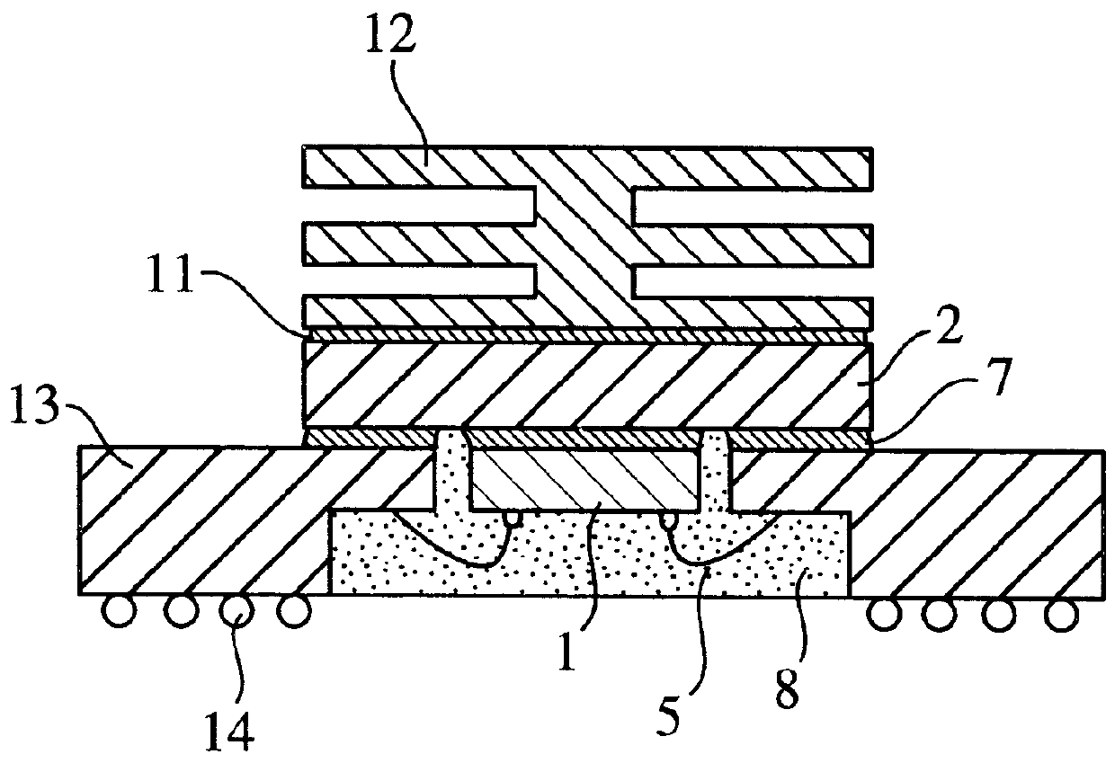
is a stepped composite heat spreader composed of two integrated stripe-pattern laminates in which t.sub.1 / t.sub.2 =1 / 1.5, t.sub.1 +t.sub.2 =1.5 mm. Example 8 is a composite heat spreader composed of two integrated stripe-pattern laminates in which t.sub.1 =t.sub.2, and t.sub.1 +t.sub.2 =1.5 mm. In both of Examples 5 and 8, two integrated stripe-pattern laminates were bonded together in a manner shown in FIGS. 20(e) and (g), and each heat spreader was covered by a plastic package as shown in FIG. 15.

The heat spreaders of Examples do not suffer from failure and damage in chips, resins and solders and are free from peeling between the Fe--Ni alloy sheets and the Cu-group metal sheets. With respect to Example 3, in which d is outside the range of 0.1-2.0 mm, .alpha. is outside the range of 0.05-1.0 mm, and b is outside the range of 0.05-1.0 mm, there are solder fatigue, resin peeling and insufficient heat dissipation because d is too large, though these problems are tolerable for some ...

example 7

A Cu-covered integrated stripe-pattern laminate 138 was produced by the method shown in FIG. 21. In the step (a), 0.15-mm-thick sheets 21 of an 36% Ni--Fe alloy and 0.2-mm-thick sheets 22 made of pure copper (commercially available) were used. A steel pipe 50 of a rectangular cross section was 10 mm in thickness, 350 mm.times.350 mm in outer size and 1500 m in length. The steel pipe 50 was lined with a 10-mm-thick Cu sheet, and an alternate laminate of the above sheets was introduced into the steel pipe 50. A lid 35 composed of an outer steel layer 51 and an inner copper layer 52 was welded to each opening of the steel pipe 50 to provide a capsule 41, which was then evacuated as shown in FIG. 21(b). The sheets were bonded together by HIP at 900.degree. C. and 1200 atms for 2 hours. The outer steel layer 51 was removed from the HIPed capsule 41 to provide a slab 30 composed of the Fe--Ni alloy sheets 21 and the Cu sheets 22 as shown in FIG. 21(c). The slab 30 was rolled by rolls disp...

example 8

Stripe-pattern laminated metal bodies produced in the same manner as in Example 1 from 0.15-mm-thick sheets 21 of 36% Ni--Fe alloy and 0.2-mm-thick pure Cu sheets 22 were observed by an optical microscope. FIG. 25 is an optical photomicrograph (.times.200) of the bonding boundary between the 36% Ni-Fe alloy and the pure Cu.

As is clear from FIG. 25, Cu is diffused into the Fe--Ni alloy. Such a diffusion region is indispensable to achieve a highly reliable integrated laminate for a heat spreader. Therefore, the hot isostatic pressing is combined with the rolling in the present invention.

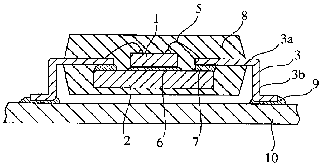
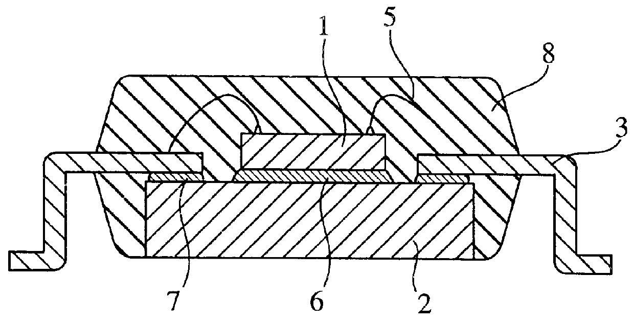
Since the heat spreader of the present invention is composed of an integrated stripe-pattern laminate of Fe--Ni alloy sheets and Cu-group metal sheets, with Cu-group metal sheets penetrating from a chip-mounting surface to an opposite surface, it is excellent in heat dissipation. Moreover, by adjusting the ratio of the Fe--Ni alloy sheets to the Cu-group metal sheets, it is possible to control the ther...


PUM

PropertyMeasurementUnit
temperatureaaaaaaaaaa
cross angleaaaaaaaaaa

Abstract

A heat spreader for a semiconductor device is constituted by an integral laminate of alternatingly stacked and diffusion-bonded Fe-Ni alloy sheets and copper-group metal sheets, the laminate having a one-directional stripe pattern of the Fe-Ni alloy sheets and the copper-group metal sheets, which appears on a planar surface on which a silicon chip is disposed. It is produced by (a) alternatingly stacking Fe-Ni alloy sheets and copper-group metal sheets, (b) hot isostatic-pressing the resulting stack of the metal sheets to form a slab, (c) rolling the slab vertically to the laminating direction of the metal sheets to form an integrated stripe-pattern laminate, and (d) cutting the integrated stripe-pattern laminate to a predetermined shape.

Description

The present invention relates to a heat spreader for semiconductor devices with excellent heat dissipation and a small difference in thermal expansion from an Si chip without peeling from a resin or ceramic package even at larger heat generation due to higher integration of chip circuits, a semiconductor device including such a heat spreader, and a method for producing such a heat spreader.Since more and more heat is generated from semiconductor devices due to increasingly higher integration of circuits, semiconductor devices are provided with heat spreaders to dissipate heat therefrom. A typical example of such semiconductor devices is shown in FIGS. 1-5. FIG. 1 shows a semiconductor device in which a silicon chip 1 is bonded to a heat spreader 2 with a bonding material layer 6 and embedded in a resin (plastic) 8. A plurality of leads of the semiconductor device are connected to a circuit board 10 via a solder layer 9. The heat of the silicon chip 1 is conducted to the heat spreade...

Claims


Application Information

Patent Timeline
Patent Type & Authority Patents(United States)
IPC IPC(8): H01L23/34H01L23/495H01L23/433H01L23/48H01L23/373
CPCH01L23/3733H01L23/4334H01L23/4951H01L24/29H01L2224/48091H01L2224/48227H01L2224/48247H01L2224/48465H01L2224/49109H01L2224/73265H01L2924/01029H01L2924/01078H01L2924/01079H01L2924/15311H01L2924/15312H01L2924/1532H01L2924/16195H01L24/48H01L2224/32245H01L2924/01322H01L2924/0132H01L24/49H01L2224/4826H01L2224/73215H01L2224/29111H01L2224/29139H01L2924/10253Y10T428/12632Y10T29/49366Y10T29/4935Y10T29/49393Y10T428/12917H01L2924/00014H01L2924/00H01L2924/0105H01L2924/01014H01L2924/01015H01L2924/01026H01L2924/01028H01L2924/01042H01L2924/01074H01L2924/01082H01L2924/3512H01L2924/14H01L2924/15787H01L2924/351H01L2224/45099H01L2224/05599H01L2224/85399H01L2224/45015H01L2924/207
Inventor OKIKAWA, SUSUMUKITAGUCHI, SABUROU
Owner HITACHI METALS LTD
Why Eureka
Try Eureka