Process for reducing copper oxide during integrated circuit fabrication

a technology of integrated circuits and copper oxides, applied in the direction of electrical equipment, decorative surface effects, decorative arts, etc., can solve the problems of aluminum, which is not suitable for large-scale integration (lsi) level technology, and is not suitable for large-scale integration (lsi) level technology, and achieves the limit of very large-scale integration (vlsi, aluminum is electromigration)

Inactive Publication Date: 2000-03-07
ADVANCED MICRO DEVICES INC
View PDF5 Cites 120 Cited by
  • Summary
  • Abstract
  • Description
  • Claims
  • Application Information

AI Technical Summary

Problems solved by technology

Aluminum, however, does have disadvantages for certain applications.
First, the electrical contact of aluminum with silicon while adequate for large scale integration (LSI) level technology, has reached its limit in the very large scale integration (VLSI) area.
Another disadvantage associated with aluminum is electromigration.
Electromigration occurs over time and may not show up until a device has had many hours of operation.
Electromigration becomes more worrisome as the level of integration increases.
Accordingly, as integrated circuit patterning schemes continue to miniaturize into the submicron dimensions, aluminum-based metallurgies will become increasingly marginal for handling the increased circuit speed and current density requirements.
However, a primary problem with integrating copper metal into multilevel metallization systems is the difficulty of patterning the metal using etching techniques.
For devices of submicron minimum feature size, wet etch techniques for copper patterning have not been acceptable due to a) liquid surface tension, b) isotropic etch profile, and c) difficulty in over-etch control.
A drawback of patterning the copper by polishing is the formation of a layer of copper oxide on the exposed copper surface.

Method used


Image

  • Process for reducing copper oxide during integrated circuit fabrication
  • Process for reducing copper oxide during integrated circuit fabrication
  • Process for reducing copper oxide during integrated circuit fabrication

Examples


Embodiment Construction

In the drawings, depicted elements are not necessarily drawn to scale and alike and similar elements may be designated by the same reference numerals through several views.

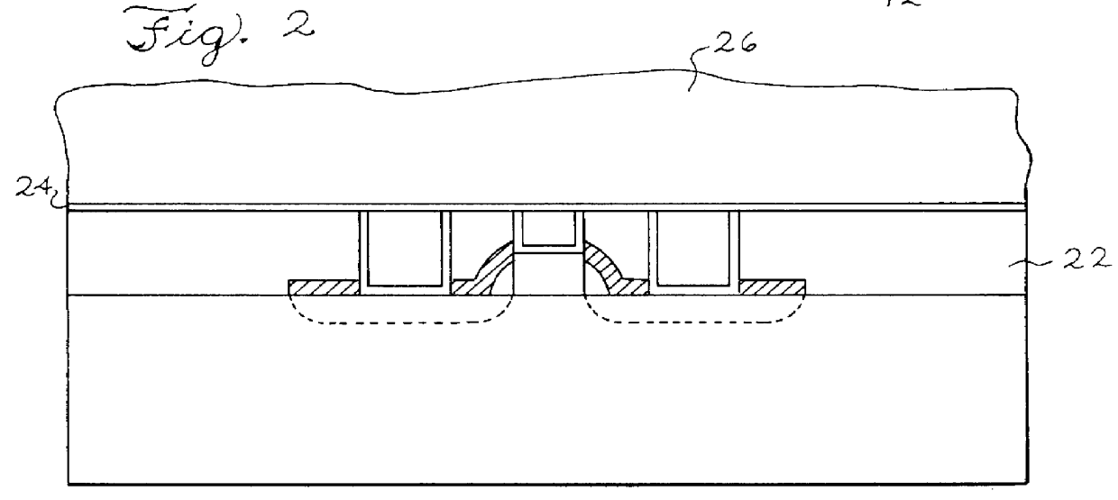
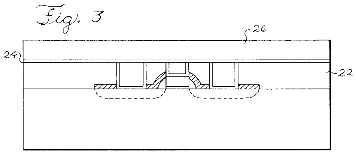
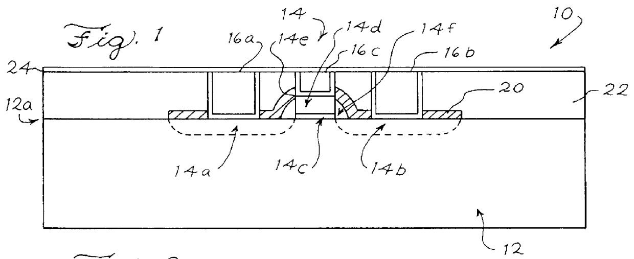
The present inventors have discovered that when copper is used for a multilevel interconnect structure of a semiconductor device and the copper is patterned using CMP, a layer of copper oxide forms on a polished surface of copper. This oxide, if not removed before another metal layer is formed over the copper, creates an increase in contact resistance and creates adhesion problems which are not desirable. The present invention overcomes these problems by reducing the amount of copper oxide present and thereby improving contact resistance and also improving adhesion between the copper layer and the copper diffusion layer silicon nitride.

FIGS. 1 to 10 and 15 are simplified sectional diagrams illustrating a process for fabricating a portion of a semiconductor device according to the present invention. The detailed co...


PUM

PropertyMeasurementUnit
pressureaaaaaaaaaa
pressureaaaaaaaaaa
RF poweraaaaaaaaaa

Abstract

A method of integrated circuit fabrication creating copper interconnect structures wherein the formation of copper oxide is reduced or eliminated by etching away the copper oxide performing an H2 plasma treatment in a plasma enhanced chemical vapor deposition chamber.

Description

FIELD OF THE INVENTIONThis invention relates to integrated circuit fabrication and more particularly to a process for reducing copper oxide by performing an H.sub.2 plasma treatment in a plasma enhanced chemical vapor deposition.DESCRIPTION OF RELEVANT ARTMetal films are utilized in semiconductor technology to wire together various components formed on a semiconductor wafer. These wires are called interconnects. Metal in semiconductor processing can also be used to function as gate electrodes in MOS structures, and as electrodes in thin film capacitors. Elemental aluminum and its alloys have been the traditional metals utilized. Advantages of aluminum include its low resistivity, superior adhesion to S.sub.i O.sub.2, ease of patterning, and high purity.Aluminum, however, does have disadvantages for certain applications. First, the electrical contact of aluminum with silicon while adequate for large scale integration (LSI) level technology, has reached its limit in the very large sca...

Claims


Application Information

Patent Timeline
Patent Type & Authority Patents(United States)
IPC IPC(8): H01L21/70H01L21/768H01L21/02H01L21/311
CPCH01L21/31122H01L21/76838
Inventor NGO, MINH VANMORALES, GUARIONEXNOGAMI, TAKESHI
Owner ADVANCED MICRO DEVICES INC
Why Eureka
Try Eureka