Lead frame, method for partial noble plating of said lead frame and semiconductor device having said lead frame
Inactive Publication Date: 2000-03-07
DAI NIPPON PRINTING CO LTD
View PDF22 Cites 107 Cited by
Summary
Abstract
Description
Claims
Application Information
AI Technical Summary
This helps you quickly interpret patents by identifying the three key elements:
Problems solved by technology
Method used
Benefits of technology
Problems solved by technology
In recent years, however, also in the case of the copper alloy lead frame as treated above, delamination of the package created in the step of assembling a semiconductor device and the step of mounting has become a problem.
This phenomenon is disadvantageous because it deteriorates the reliability of IC and the percentage non-defective in the step of IC assembly and the step of mounting.
The delamination of the copper alloy lead frame is considered attributable to the fact that an oxide film is formed on the surface of the copper alloy in the step of heat treatment in the course of IC assembly, the strength of bond between the formed oxide film and the metal being unsatisfactory.
In this lead frame, however, since the silver plated area also is covered with the coating of other metals, stable gold wire bonding cannot be achieved.
Method used
Image
Click on the blue label to locate the original text in one second.
Reading with bidirectional positioning of images and text.
Examples
example 1
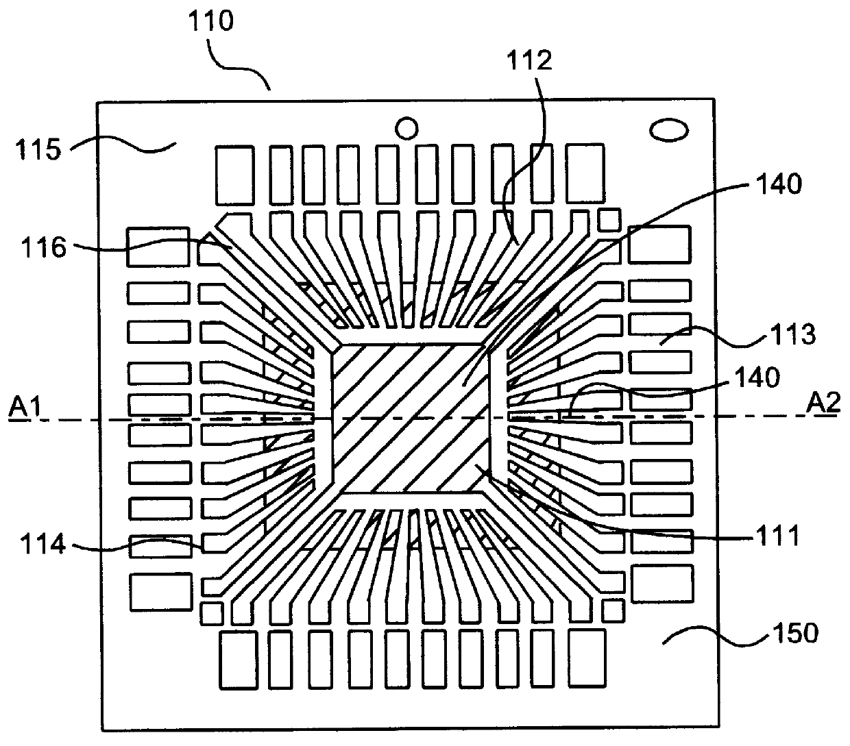
FIG. 1 shows an embodiment of the lead frame of the present invention, wherein FIG. 1 (b) is a plan view of the lead frame and FIG. 1 (a) is an enlarged view of the principal part in section taken on line A1-A2 of FIG. 1 (b).
In FIG. 1, numeral 110 designates a lead frame, numeral 111 a die pad, numeral 112 an inner lead, numeral 113 an outer lead, numeral 114 a dam bar, numeral 115 a frame, numeral 116 a supporting bar, numeral 120 a lead frame material (a copper alloy), numeral 130 a copper plating, numeral 140 a partial silver plating, and numeral 150 a thin silver plating.
In the lead frame 110, a 0.15 mm-thick copper alloy material (EFTEC64T-1 / 2H material, manufactured by The Furukawa Electric Co., Ltd.) is etched to prepare a lead frame material 120 having an external shape as shown in FIG. 1 (b), the whole surface of the lead frame material 120 is plated with copper 130, and only a predetermined area of the copper plating 130 is plated with silver to form a partial silver plati...
example 2
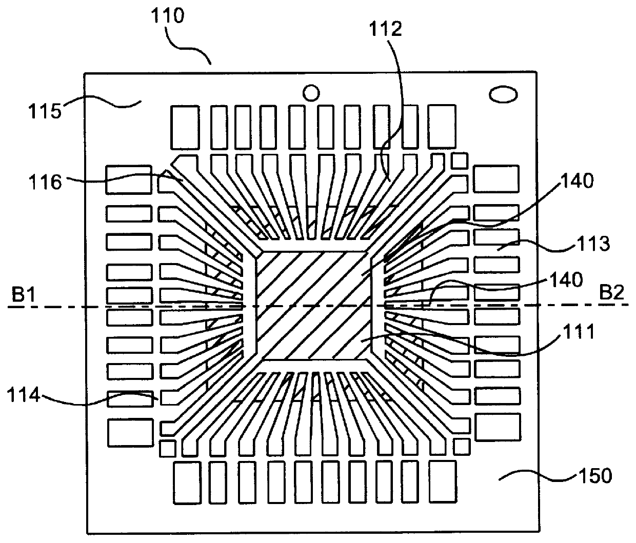
FIG. 2 shows an embodiment of the lead frame of the present invention, wherein FIG. 2 (b) is a plan view of the lead frame and FIG. 2 (a) is an enlarged view of the principal part in section taken on line B1-B2 of FIG. 2 (b).
In FIG. 2, numeral 110 designates a lead frame, numeral 111 a die pad, numeral 112 an inner lead, numeral 113 an outer lead, numeral 114 a dam bar, numeral 115 a frame, numeral 120 a lead frame material (a copper alloy), numeral 130 a copper plating, numeral 140 a partial silver plating, and numeral 150 a thin silver plating.
In the lead frame 110, a 0.15 mm-thick copper alloy material (EFTEC64T-1 / 2H material, manufactured by The Furukawa Electric Co., Ltd.) is etched to prepare a lead frame material 120 having an external shape as shown in FIG. 1 (b), the whole surface of the lead frame material 120 is plated with copper 130, and the whole surface of the copper plating is plated with silver to form a thin silver plating 150, and, further, a predetermined area of...
example 3
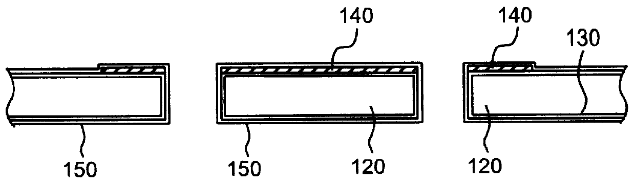
A process for partially plating a lead frame according to the present invention will be described with reference to FIG. 3. This example demonstrates a process for producing the lead frame of Example 1.
A lead frame 120 of a shaped copper alloy, which has been pretreated for plating, Was first provided (FIG. 3 (a)), and the whole surface thereof was plated with copper to form a 0.1 .mu.m-thick copper plating 130 (FIG. 3 (b)).
In the pretreatment for plating, the whole surface of the lead frame 120, made of a copper alloy, shaped by etching was electrolytically degreased, washed with pure water, and subjected to acid activation treatment for removing the oxide film, formed on the surface of the frame, with an acidic solution, thereby activating the surface of the copper alloy as a lead frame material 120, and again washed with pure water.
Copper plating was performed using copper cyanide at a bath temperature of 50.degree. C. for about 20 sec to a thickness of about 0.1 .mu.m.
Subsequent...
PUM
Abstract
A lead frame for a semiconductor device, made of a copperalloy, capable of preventing the creation of delamination between encapsuling resin and attributable to a lead frame without sacrificing the wire bondability and, a process for producing the lead frame and a semiconductor device using the lead frame. According to the present invention, (1) there is provided a lead frame for a plastic molded type semiconductor device, made of a copperalloy material partially plated with at least one noble metal, for wire bonding or die bonding purposes, selected from silver, gold, and palladium, wherein the whole area or a predetermined area of the surface of the copper at least on its side to be contacted with a encapsuling resin has a thin noble metal plating of at least one member selected from silver, gold, platinum, and palladium. (2) A copper strike plating is provided as a primer plating for the partial noble plating, a copper plating is provided on the thin noble metal plating, and the partial noble metal plating is provided on the copper plating in its predetermined area. (3) A die pad for mounting a semiconductor chip is provided, a partial silver plating is provided, and a zinc flash plating and a copper strike plating are provided in that order at least one on the surface of copper in the back surface of the die pad remote from the surface on which the semiconductor chip is mounted.
Description
The present invention relates to a lead frame for a semiconductor device, and more particularly to a lead frame, made of a copper alloy material, improved particularly in strength of bond to a sealing resin.DESCRIPTION OF THE PRIOR ARTA conventional plastic molded type semiconductor device (a plastic lead frame package) generally has a structure as shown in FIG. 20(a). Specifically, it comprises a die pad section 1011 for mounting thereon a semiconductor chip 1020, an outer lead section 1013 for electrical connection to a peripheral circuit, an inner lead section 1012 integral with the outer lead section 1013, a wire 1030 for electrically connecting a front end of the inner lead section 1012 to an electrode pad (a terminal) 1021 of a semiconductor chip 1020, a resin 1040 for sealing the semiconductor chip 1020 to protect the semiconductor chip 1020 against stress and contamination from an external environment, and the like. After the semiconductor chip 1020 is mounted on the die pad...
Claims
Application Information
Patent Timeline
Application Date:The date an application was filed.
Publication Date:The date a patent or application was officially published.
First Publication Date:The earliest publication date of a patent with the same application number.
Issue Date:Publication date of the patent grant document.
PCT Entry Date:The Entry date of PCT National Phase.
Estimated Expiry Date:The statutory expiry date of a patent right according to the Patent Law, and it is the longest term of protection that the patent right can achieve without the termination of the patent right due to other reasons(Term extension factor has been taken into account ).
Invalid Date:Actual expiry date is based on effective date or publication date of legal transaction data of invalid patent.

