Short turn around time mask ROM process

a mask rom and short turn around time technology, applied in the field of information storage, can solve the problems of unacceptably long turn around time, unacceptably high flash memory cost, and increase the cost of the mask rom,

Inactive Publication Date: 2000-04-25
UNITED MICROELECTRONICS CORP
View PDF3 Cites 29 Cited by
  • Summary
  • Abstract
  • Description
  • Claims
  • Application Information

AI Technical Summary

Problems solved by technology

Such ROMs have undesirably long turn around times. Non-volatile memories such as flash memories can be programmed after all processing is done on the device and so have short turn around times. Flash memories, however, are unacceptably expensive in comparison to mask ROMs.
For 0.5 .mu.m design rules, such as are implemented in some current memory designs, alignment of the implantation mask is a time consuming and error prone process which increases t...

Method used


Image

  • Short turn around time mask ROM process
  • Short turn around time mask ROM process
  • Short turn around time mask ROM process

Examples


Embodiment Construction

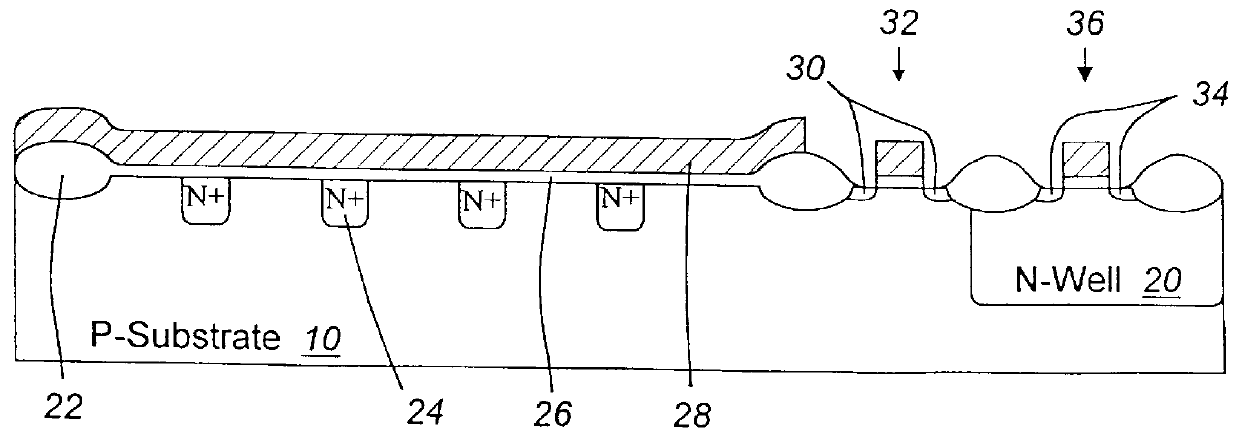
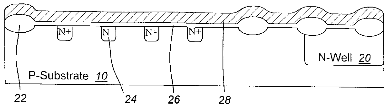
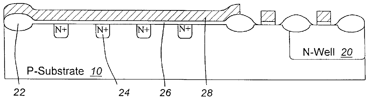
An aspect of the present invention provides a method of programming a mask ROM comprising forming an encoding mask on an insulating layer formed over a structure consisting of memory transistors each having a gate, wherein the encoding mask provides a plurality of openings corresponding to possible memory locations within the mask ROM. Programming is accomplished by implanting impurities through the openings in the encoding mask and through the insulating layer into the gates of the memory transistors and then removing the encoding mask.

A more specific aspect of this invention includes steps of blanket doping a layer of polysilicon with a first dopant of a first conductivity type, wherein the step of programming locally alters the polysilicon to a second conductivity type by adding to the polysilicon layer second dopants of the second conductivity type.

Another aspect of the present invention provides a method of programming a mask ROM by providing a substrate covered with a gate oxi...


PUM


Abstract

A mask ROM stores information by selecting the work function of the gates of each FET in an array of FETs at a late stage in the manufacture of the ROM. The polysilicon gates of some of the FETs are doped N-type and the gates of the other FETs are doped P-type to form gates having different work functions, thereby forming FETs having different threshold voltages. The ROM consists of a parallel array of buried N+ bit lines formed in the substrate, a gate oxide layer deposited over the bit lines and a layer of polysilicon deposited on the gate oxide. The polysilicon is blanket doped N-type, gate electrodes are defined by photolithography, and then self-aligned silicide layers are formed on the gate electrodes. An insulating layer is then formed over the gate electrodes. Programming of the ROM is accomplished by forming a mask on the insulating layer and then implanting ions through openings in the mask, through the insulating layer and the silicide layer, and into the polysilicon layer. The implantation converts individual gate electrodes from N-type to P-type to alter the threshold voltage of the selected transistors. Relatively few additional processing steps are needed after the programming to complete the ROM.

Description

1. Field of the InventionThe present invention relates to the storage of information by altering the operational characteristics of a transistor within an array of memory transistors and, more particularly, to a non-volatile memory such as a read only memory (ROM).2. Description of the Related ArtConventional read only memories (ROMs) consist of an array of field effect transistors, with each memory cell including a single field effect device. Each of the field effect transistors can be formed so as to have one of two predetermined values of a particular characteristic of the transistor. The selectable transistor characteristic might, for example, be the threshold voltage of the transistor. Implanting impurities into the channel region of the transistor might cause the transistor to have a low threshold voltage so that the transistor is turned on by application of V.sub.CC to the gate of the transistor. Transistors formed without implanting impurities into the channel might have a h...

Claims


Application Information

Patent Timeline
IPC IPC(8): H01L21/70H01L21/8246
CPCH01L27/11293H01L27/1126H10B20/383H10B20/65
Inventor SHEU, SHING-RENKUNG, CHENG-CHIH
Owner UNITED MICROELECTRONICS CORP
Why Eureka
Try Eureka