Pattern inspection method and system

Inactive Publication Date: 2000-05-16
FUJITSU SEMICON LTD
View PDF4 Cites 41 Cited by
  • Summary
  • Abstract
  • Description
  • Claims
  • Application Information

AI Technical Summary

Benefits of technology

It is an object of the present invention to provide a defect inspection method capable of inspecting a defect of a pattern in a short time and providing a practically sufficient precision.
By extracting patterns of a specific configuration from image data, inspection of the image data, etc. is made easy.
As above, patterns can be inspected at high sensitivity and with high reliability in a short time.

Problems solved by technology

Even fine defects may affect circuit performance because patterns are becoming very narrow.
A fine pattern actually formed by using a designed pattern becomes different from the designed pattern because of interferences of light in lithography process or the like during manufacture.
However, these corners are not real defects but are within allowance.
Such defects will be called quasi defects.
Various types of processes including the rounding process are therefore required in detecting detects by comparison between a formed pattern and data in a database, so that it takes a long time to carry out defect inspection.
However, for example, if a designed pattern itself has a defect or if dust is attached to the reticle during exposure and the same pattern with the dust defect is exposed to a number of dies, such defects cannot be detected by the same pattern comparison inspection.
However, comparison between different kind of patterns, such as data in a database and a pattern on a reticle, may result in a quasi defect described above if it is performed at high defect detection sensitivity, and a long time is required for a defect inspection work.
Although the die-to-die comparison inspection and the die-to-database comparison inspection can be performed concurrently, the comparison inspection process takes a long time because the image data in the database is different in representation from the image data of the die.
With an increase in integration density of a semiconductor integrated circuit device, the patterns thereof become complicated.
There may occur such mistakes in the stage of designing the patterns that patterns which should be formed are omitted, and that patterns which should not be formed are formed.
In such cases, the database itself includes mistakes.
When masks or semiconductor wafers faithful to such a database are formed, however, those mistakes cannot be detected by usual defect or fault inspection.
A long time inspection becomes necessary to detect and correct such mistakes.
In the case of automatically generating patterns in this way, however, patterns may be forcedly generated at positions where the patterns should not be formed.

Method used


Image

  • Pattern inspection method and system
  • Pattern inspection method and system
  • Pattern inspection method and system

Examples


Embodiment Construction

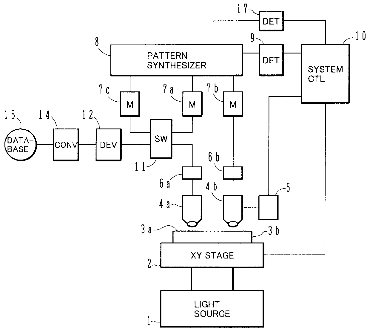
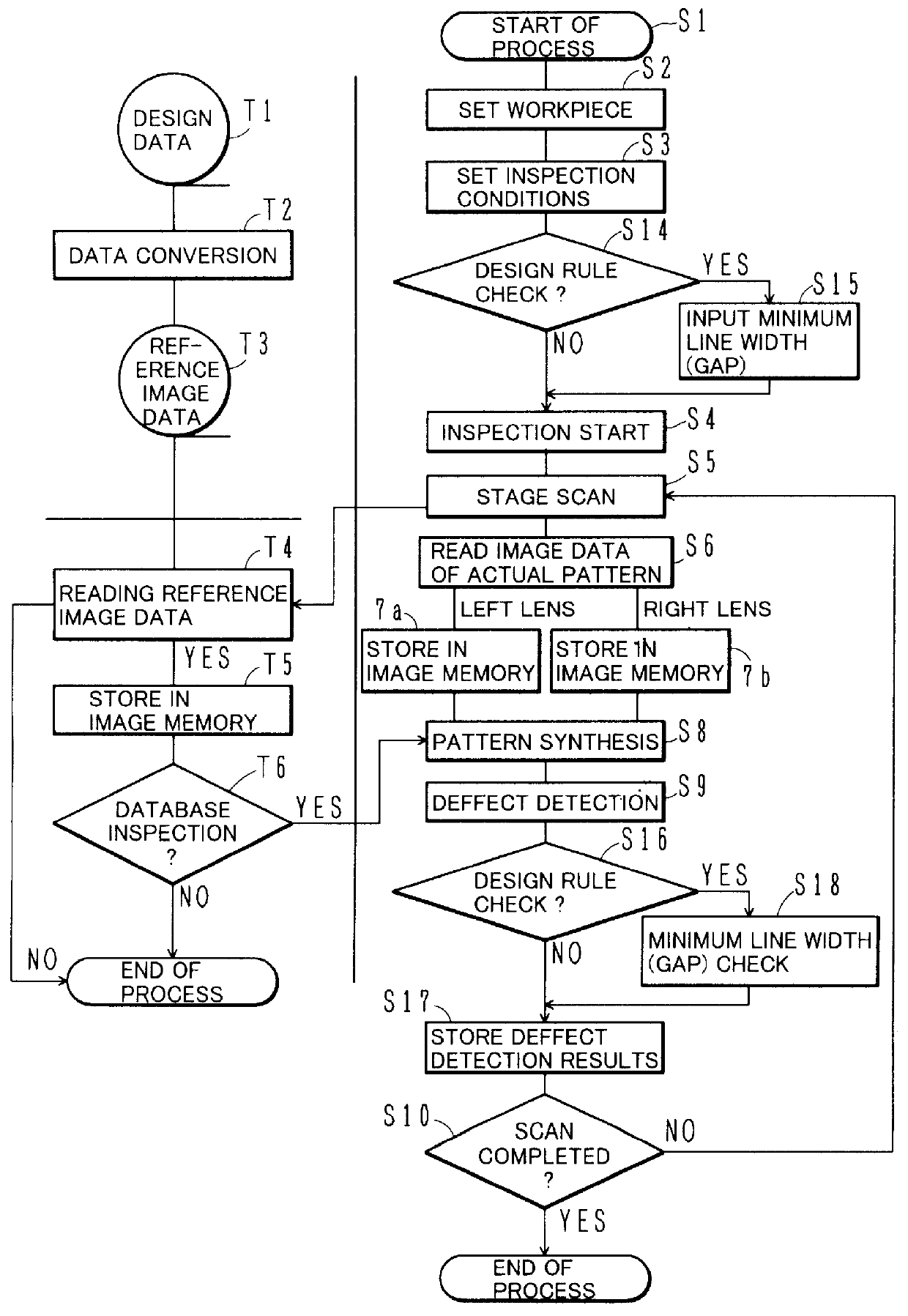
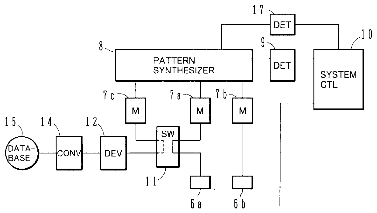
FIG. 1 is a block diagram showing the structure of a defect inspection apparatus according to an embodiment of the invention. Illumination light from a light source 1 is applied to an inspection workpiece 3 (3a, 3b) placed on an XY stage. The inspection workpiece 3a, 3b may be a semiconductor wafer having a plurality of inspection areas or a pair of masks (including reticles) having the same pattern. The inspection workpiece may also be a glass substrate of a liquid crystal display. It may be any fine pattern formed on or in a substrate and requiring inspection.

A pair of object optical systems 4a and 4b are disposed above the inspection workpiece 3a, 3b. A pair of light reception elements 6a and 6b are placed on the image surfaces of the object optical systems 4a, 4b. The light reception elements 6a, 6b may be line sensors made of CCDs. The focus of the object optical systems 4a, 4b are adjusted by an automatic focussing mechanism 5. The inspection workpiece 3a, 3b can be two-dimens...


PUM


Abstract

A pattern inspection method includes the steps of: obtaining first image data by optically picking up an actually formed pattern such as a reticle; aligning a position of the first image data with second image data of a pattern at a different layer from that of the first image data; and performing a first pattern inspection using the first and second image data. Defect inspection can be executed in a short time with a practically sufficient precision.

Description

This application is based on Japanese patent applications 8-56474 and 9-51957, filed on Mar. 13, 1996 and Mar. 6, 1997, all the contents of which are incorporated herein by reference.BACKGROUND OF THE INVENTIONa) Field of the InventionThe present invention relates to pattern defect inspection, and more particularly to inspection of a defect of a pattern formed on reticles, photomasks, or wafers, or of a database representing a pattern.b) Description of the Related ArtVarious patterns are formed on semiconductor wafers during manufacture of semiconductor devices. Generally, a reticle or mask having a pattern of an original layout is optically transferred in a reduced size or in the same 1:1 size to a resist layer coated on a semiconductor wafer, and developed to form a resist mask. By using this resist mask as a process mask, the underlying layer is processed.A plurality of photolithography processes are generally carried out for the completion of a single semiconductor device. A mas...

Claims


Application Information

Patent Timeline
IPC IPC(8): G01B11/00H01L21/66
CPCG01B11/00G06T2207/30148G06T7/001G01N21/95607G06T7/0006H01L22/00
Inventor KOBAYASHI, KEN-ICHIMATSUYAMA, TAKAYOSHIMATSUI, SHOWGO
Owner FUJITSU SEMICON LTD
Why Eureka
Try Eureka