
Method of writing cross pattern in adjacent areas of layer sensitive to charged particle beam for improving stitching accuracy without sacrifice of throughput

a technology of charged particle beam and cross pattern, which is applied in the field of charging particle beam lithography, can solve the problems of low stitching accuracy, pattern deformation, and serious shortage of current density, and achieve the effect of improving stitching accuracy

Inactive Publication Date: 2000-05-23
NEC ELECTRONICS CORP
View PDF6 Cites 5 Cited by
  • Summary
  • Abstract
  • Description
  • Claims
  • Application Information

AI Technical Summary

Benefits of technology

It is therefore an important object of the present invention to provide a method of writing a cross pattern, which is improved in stitching accuracy without sacrifice of the throughput of a charged particle beam lithographic machine.

Problems solved by technology

When the prior art variable shaped electron beam lithography machine is used for a miniature pattern equal to or less than 0.25 micron wide, the pattern deformation due to the low stitching accuracy and the shortage of current density is serious, and reduces the production cost.
manufacturer suffers from a low stitching accuracy.
The sub-pattern 7d is so short that the manufacturer suffers from not only a low stitching accuracy but also deformation of the latent image due to shortage of current density.
The multiple pattern transfer consumes long time, and the manufacturer suffers from a low throughput.
However, when there are cross patterns, a controller is required to rearrange the patterns to be written into the sub-fields, and consumes long time.

Method used


Image

  • Method of writing cross pattern in adjacent areas of layer sensitive to charged particle beam for improving stitching accuracy without sacrifice of throughput
  • Method of writing cross pattern in adjacent areas of layer sensitive to charged particle beam for improving stitching accuracy without sacrifice of throughput
  • Method of writing cross pattern in adjacent areas of layer sensitive to charged particle beam for improving stitching accuracy without sacrifice of throughput

Examples


first embodiment

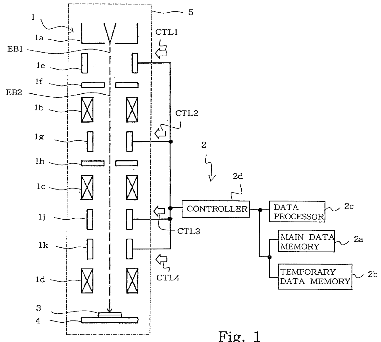
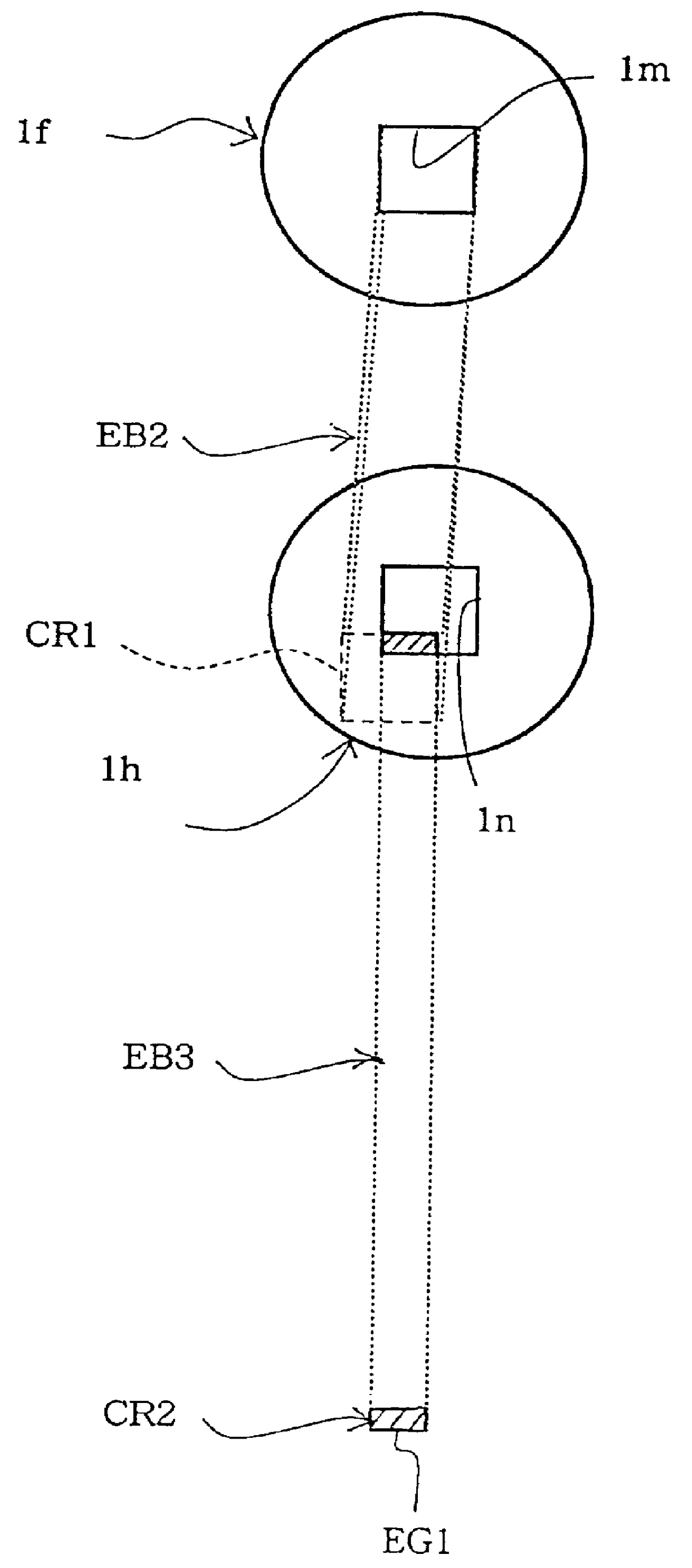
FIG. 7 illustrates a program sequence for a method embodying the present invention. The method implementing the first embodiment is realized by a charged particle beam lithographic machine similar to the lithographic machine shown in FIG. 1. For this reason, no description is made on the charged particle beam lithographic machine, and components of the lithographic machine are specified by using the references designating corresponding components of the variable shaped electron beam lithographic machine shown in FIG. 1, if necessary. In this instance, the first aperture plate 1f, the beam shaping deflector 1g and the second aperture plate 1h as a whole constitute a beam shaping means. The main deflector 1j deflects each shot of charged particle beam over a layer sensitive to the charged particle beam, and the sub-deflector 1k defects each shot in a sub-field.

Latent images 11, 12 and 13 of three different cross patterns are formed in adjacent sub-fields 14 and 15 of a charged particl...

second embodiment

FIG. 9 illustrates another program sequence embodying the present invention. The program sequence is used in a charged particle beam lithographic machine similar to the variable shaped electron beam lithographic machine, and components of the charged particle beam lithographic machine are accompanied with the references designating corresponding components of the variable shaped electron beam lithographic machine in the following description.

FIG. 10 illustrates patterns 21 / 22 to be written into a layer 23 sensitive to a charged particle beam. The layers 23 are virtually divided into sub-fields 23a of the maximum size as indicated by broken lines. The size of the sub-fields 23a is variable, and "F" represents the length of the edge line defining the sub-field 23a. The sub-field 23a measures Fmax.times.Fmax, and Fmax is stored in the main memory 2a. In this instance, a critical length is equal to the maximum length Fmax, and is also represented by "Fmax". When the charged particle be...


PUM


Abstract

A data processor compares a length of a pattern to be written into a layer sensitive to a charged particle beam with a critical length equal to the maximum length of a cross section of the charged particle beam or the maximum length of a variable sub-field to see whether or not the pattern is written through a radiation of the maximized cross section or through a radiation onto the maximized sub-field, and a main deflector and a sub-deflector guide a shot of charged particle beam to the layer if the answer is positive so that the pattern is prevented from deformation due to a low stitching accuracy.

Description

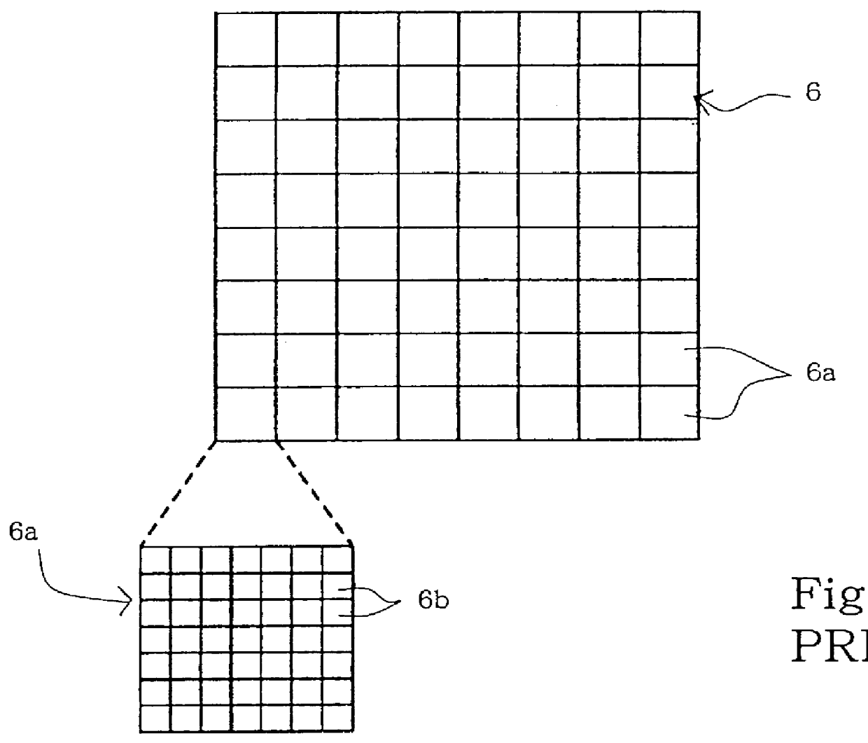
FIELD OF THE INVENTIONThis invention relates to a charged particle beam lithography and, more particularly, to a method of writing a cross pattern in adjacent areas of a layer sensitive to a charged particle beam for improving a stitching accuracy without sacrifice of the throughput.DESCRIPTION OF THE RELATED ARTAn integrated circuit device is fabricated on a semiconductor wafer through repetition of a pattern transfer from photo-masks and / or a direct pattern writing. A miniature pattern is desirable for increasing the integration density, and research and development efforts have been made on various lithographic technologies. A charged particle beam lithography is attractive to the manufacturer for transferring a miniature pattern equal to or less than 0.25 micron. An electron beam is, by way of example, used in the charged particle beam lithography.FIG. 1 illustrates a standard variable shaped electron beam lithography machine. The standard variable shaped electron beam lithograp...

Claims


Application Information

Patent Timeline
IPC IPC(8): H01J37/302H01J37/30H01L21/027
CPCH01J37/3026H01J2237/31764H01L21/027
Inventor TAMURA, TAKAO
Owner NEC ELECTRONICS CORP
Learn More