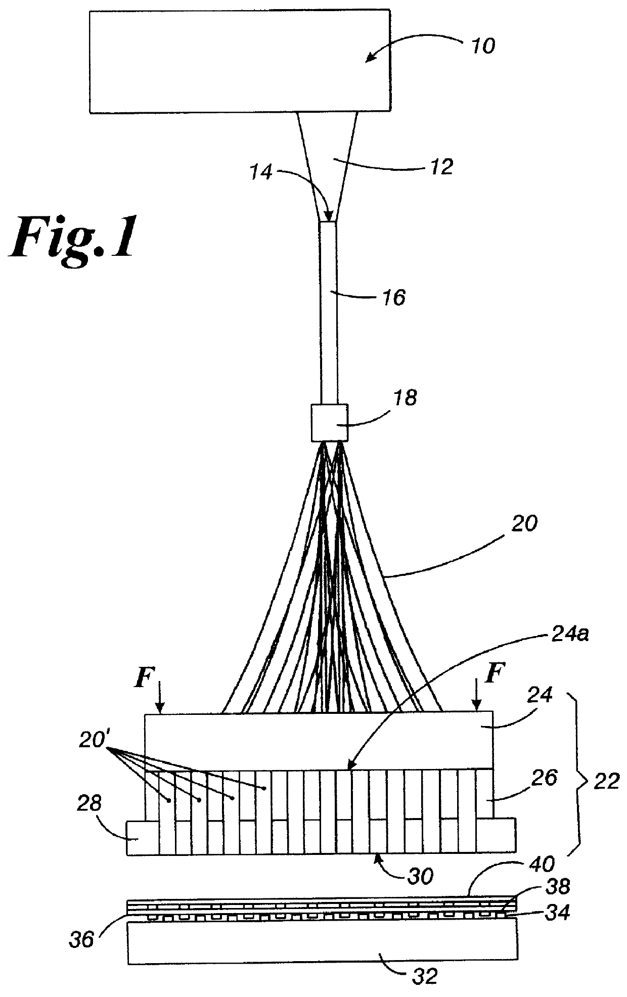
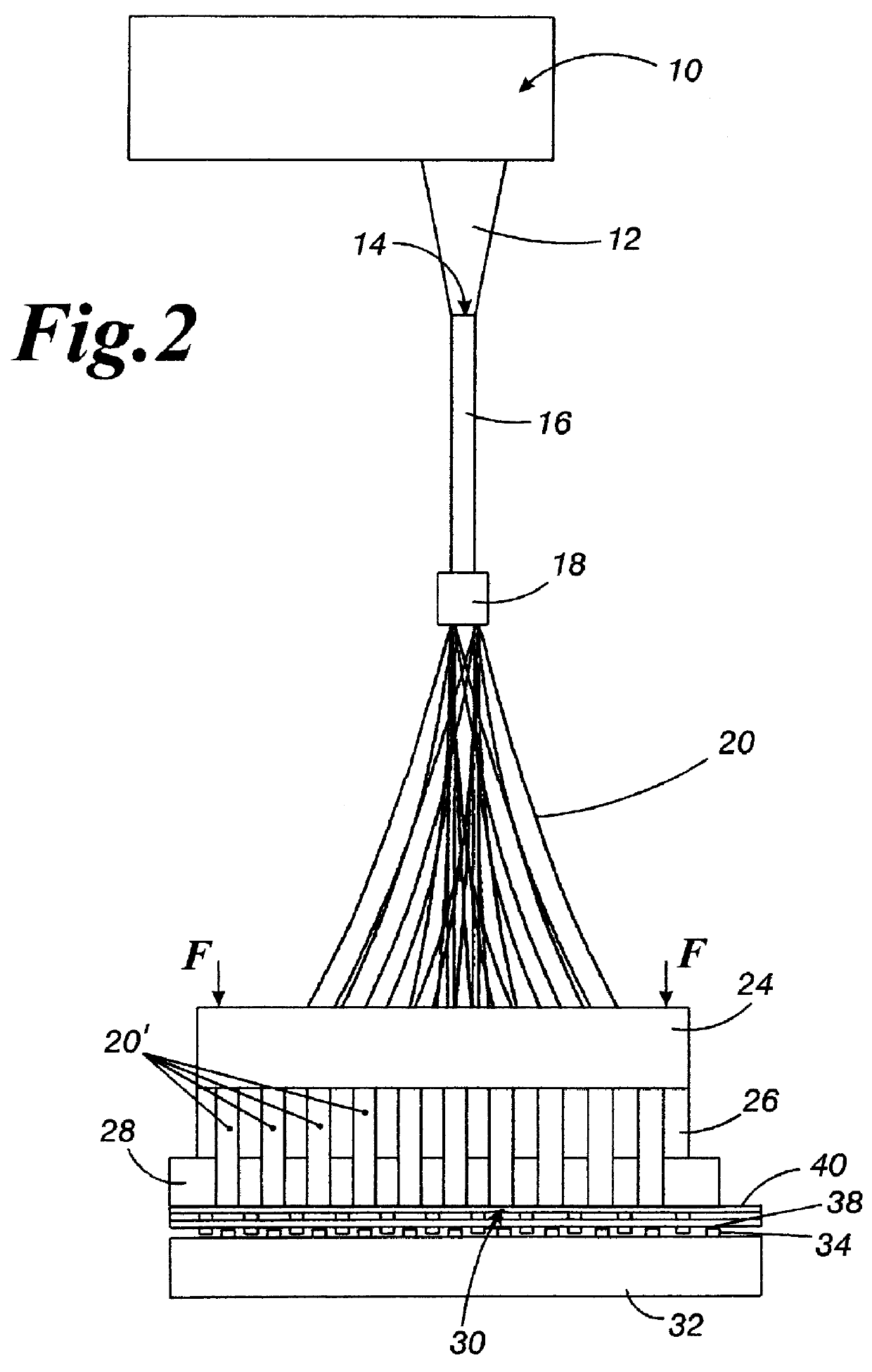
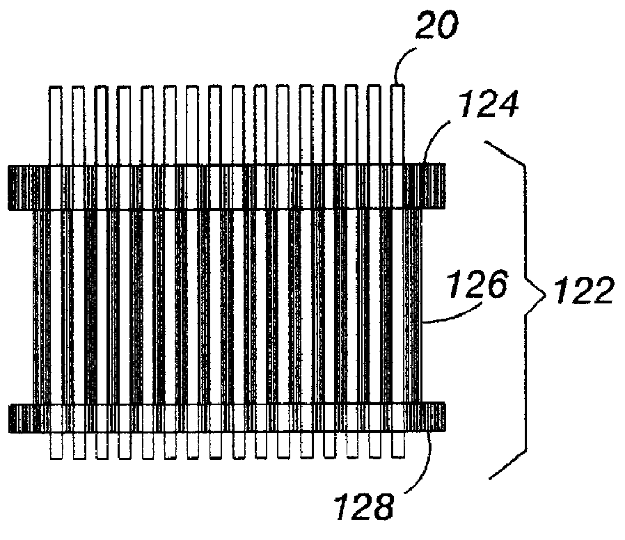
The present invention provides a device for electrically connecting contact elements by means of laser energy, said device permitting the simultaneous production of a plurality of connections in which two respective contact elements are interconnected, and said device permitting a rapid and reproducable production of connections even in the case of very small contact geometries; a uniformly high quality of the connections produced and a good exploitation and conversion of the laser energy is given. The present invention is based on the finding that a good exploitation of the laser energy is achieved when the pressure for minimizing the distance between the contact elements is applied to the connection points, i.e. the contact elements, directly through the optical fibres through which the laser energy is conducted.
In order to guarantee that the connection surfaces of all contact elements to be connected are pressed onto one another when a plurality of connections is being produced, a means for compensating different distances between the optical fibre ends and the surfaces of the contact element pairs to be connected is provided according to the present invention. It is thus possible to use the present invention for producing high-quality connections essentially simultaneously with good exploitation of the laser energy, even if the surfaces which constitute part of the contact element pairs to be connected and which face the optical fibres are not positioned precisely in one plane.
By means of the optical fibres of the connecting device according to the present invention, which conduct the laser
radiation to the points to be connected, the laser
radiation can optimally be converted into
thermal energy used for the connecting operation, i.e. for
welding or
soldering, so that unsatisfactory connection points caused by insufficient heat as well as excessive heating, which might destroy the contacts, are avoided. In view of the fact that the optical fibre ends are brought into direct contact with a surface of the contact elements to be connected, deposits which may perhaps occur at the end of an optical fibre will not influence the
coupling in of the laser energy, effected for converting said laser energy into
thermal energy used for producing the connection, to the same extent to which said
coupling in of laser energy is influenced in cases where a distance is maintained between the end of an optical fibre and the connection point. Furthermore, the pressing together of the contact elements, which is guaranteed according to the present invention for all connections even in the case of an essentially simultaneous production of a plurality of connections, will increase
thermal coupling, the effective contact surface between the individual contact elements increasing rapidly during the
soldering period; this results in optimum
thermal coupling with the contact elements to be connected.
The present invention is specially suitable for producing connections between connecting leads and solder connection surfaces on a substrate or
chip. Due to the essentially simultaneous contacting of a plurality of connection points, very short
processing times per component are possible in accordance with the present invention.
The present invention is e.g. particularly suitable for producing connections between conductors of a flexible circuit carrier and contact points of a substrate or a
chip. The flexible circuit carrier is defined by a foil which is transmissive with regard to the
wavelength of the laser
radiation used, whereby the laser energy passes through the foil almost without any losses and is absorbed and converted into heat only on the surface of the connecting lead, which consists e.g. of
copper. Due to this heat and the
contact force during the contacting process, an
electrically conductive connection is established between conductors of the flexible circuit carrier and contact points of the substrate or
chip. Further advantages are to be seen in the fact that the laser energy is converted into heat only below said flexible foil material, e.g. on a
copper conductor. Hence, problems with the heat-transmission resistance and problems with the
thermal conduction of the foil will be avoided. Furthermore, the
adhesive layers in the flexible circuit carrier will be prevented from being destroyed by excessively high temperatures.

