Polishing pad and apparatus for polishing a semiconductor wafer

a technology for polishing pads and semiconductor wafers, which is applied in the direction of gear teeth, gear teeth, gear teeth, etc., can solve the problems of difficult to uniformly polish difficult to flatten local topographies on insulating layers, and difficult to polish insulating layers in a global rang

Inactive Publication Date: 2000-06-20
TOKYO ELECTRON LTD
View PDF14 Cites 65 Cited by
  • Summary
  • Abstract
  • Description
  • Claims
  • Application Information

AI Technical Summary

Benefits of technology

Accordingly, an object of the invention is to provide a polishing pad and an apparatus for polishing a semiconductor wafer, in which the polishing pad does not have any wrinkles thereon and the semiconductor wafer can be polished uniformly over a long period of time.

Problems solved by technology

This means that it is difficult to flatten local topographies on the insulating layer.
On the other hand, when a rigid polishing pad is used, the pad tends to polish only the projected portions in the global deflection of the wafer, but not polish the local topographies uniformly.
As a result, it is difficult to polish the insulating layer uniformly in a global range.
The polishing rate at the protruded portion becomes larger locally, therefore, the wafer is not polished uniformly.
In general, the polishing pad is frequently changed to new one, therefore, the attachment accuracy of the polishing pad is not stable, and it is difficult to perform a polishing process accurately.
As a result, the polishing apparatus itself does not always work well, and the operating efficiency of the apparatus is decreased.
On the other hand, when the polishing pad is attached to the turn table by the stretch-holding technique, air bubbles do not easily get into the space between the polishing pad and the turn table.
Even though, some air bubbles get into the space, those are easily taken out.
The material, which holds the polishing slurry well, may be of foamed material having a high degree of swelling, so that the polishing pad is swelled and deformed when absorbing the polishing slurry.
When the polishing pad is swelled, the attachment between the polishing pad and the turn table gets loose.
When the wrinkles are made on the polishing pad, a part of the wafer is locally over polished, so that the entire surface of the wafer is not polished uniformly.
Especially in an apparatus that performs a dressing process of a polishing pad, the polishing pad is locally over dressed at portions where the wrinkles formed, so that the entire surface of the wafer is not polished uniformly.
In other words, specific regions of the polishing pad are locally over shaved, therefore, the polishing pad can not be used over a long period of time.

Method used


Image

  • Polishing pad and apparatus for polishing a semiconductor wafer
  • Polishing pad and apparatus for polishing a semiconductor wafer
  • Polishing pad and apparatus for polishing a semiconductor wafer

Examples


Embodiment Construction

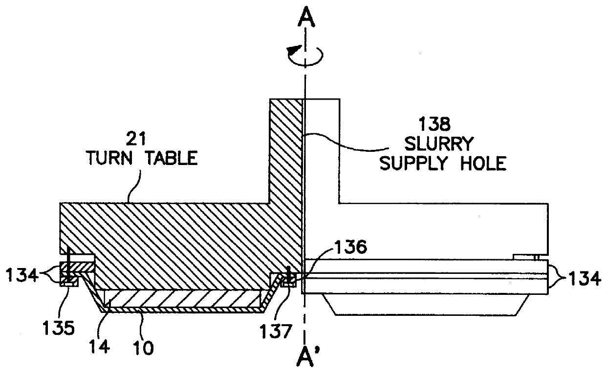
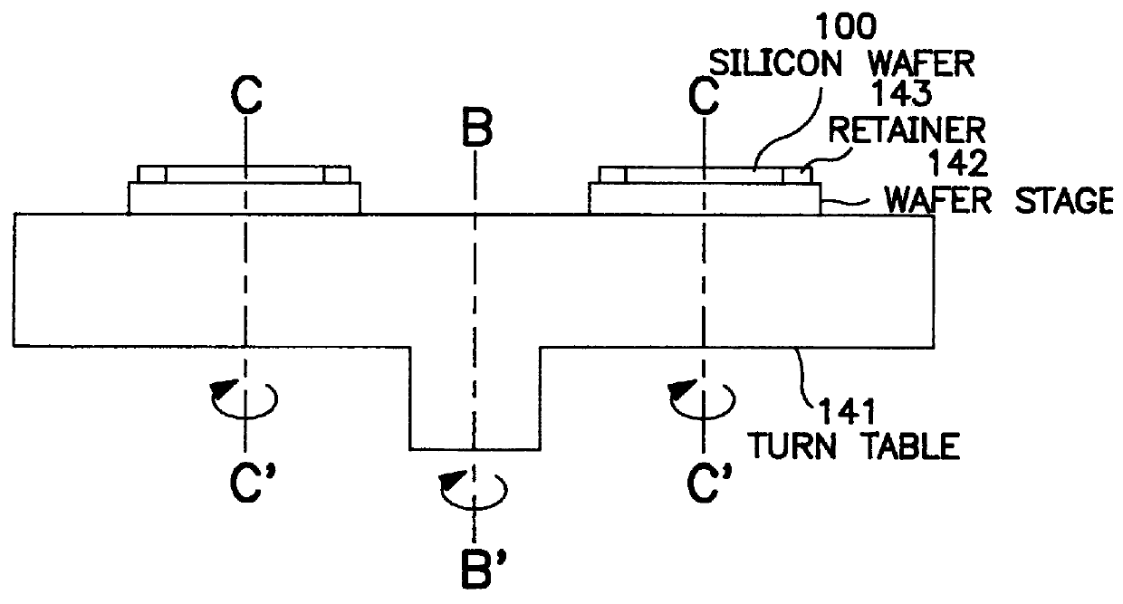
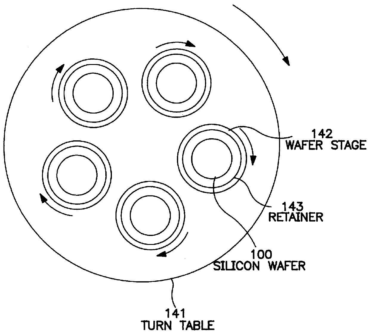
FIG. 1 shows an apparatus for polishing a silicon wafer 100, according to a first preferred embodiment of the invention. The apparatus includes a turn table 21, a polishing pad 10 attached to the turn table 21, an elastic member 14 sandwiched between the turn table 21 and the polishing pad 10, a wafer turn table 141, a wafer stage 142 and a retainer 143 holding the wafer 100.

The elastic member 14 is shaped to be a ring-shape having a center hole, and is fixed to the turn table 21 with a double-sided tape, or the like. The elastic member 14 is carefully attached to the turn table 21 so that no air bubbles get into the space between them. Basically, once the elastic member 14 is attached to the turn table 21, the elastic member 14 is not often changed to new one. The polishing pad 10 is also shaped to be a ring-shape, and is attached with inner ring 136 and periphery ring 134 and bolts 137 and 135 to the bottom of the turn table 21. The wafer stage 142 is rotatably mounted on the wafe...


PUM


Abstract

An apparatus for polishing a semiconductor wafer includes a polishing pad to be in contact with the semiconductor wafer; a turn table which rotates the polishing pad; and an elastic member which is arranged between the turn table and the polishing pad. The polishing pad includes a polishing layer which is made of a material having a good characteristic of slurry holding; and a support layer which is made of a rigid material having an optimum thickness to prevent the polishing layer from loosening. The polishing pad is attached to the turn table by a stretch-holding technique without adhesive bonding.

Description

This application claims the priority of Application No. H08-319181, filed Nov. 29, 1996 in Japan, the subject matter of which is incorporated herein by reference.The present invention relates to a polishing pad and an apparatus for polishing a flat plate object, such as a semiconductor wafer. And more particularly, the invention relates to a polishing pad and an apparatus for polishing a semiconductor wafer, in which the polishing pad is attached to a turn table with a stretch-holding technique without adhesive bonding.In general, integrated circuit (IC) devices manufactured today rely upon an elaborate system of conductive interconnects for wiring together transistors, resistors, and other IC components which are formed on a semiconductor substrate. The technology for forming these interconnects is highly sophisticated and well understood by practitioners skilled in the art. In a typical IC device manufacturing process, many layers of interconnects are formed over a semiconductor s...

Claims


Application Information

Patent Timeline
Patent Type & Authority Patents(United States)
IPC IPC(8): B24D3/28B24D3/20B24B37/04B24D13/14B24D13/00B24B37/20B24B37/22B24B37/24B24B37/26
CPCB24D3/28B24B37/26H01L21/304
Inventor FUJITA, TAKASHIKOZAI, YUZOOHARA, MOTOYUKI
Owner TOKYO ELECTRON LTD
Why Eureka
Try Eureka