

Array substrate comprising semiconductor contact layers having same outline as signal lines
a semiconductor contact layer and substrate technology, applied in the field of array substrates, can solve the problems of reducing manufacturing yield and adversely reducing aperture ratio, and achieve the effects of suppressing or eliminating a significant increase in storage capacitors, high aperture ratio, and reduced manufacturing yield
- Summary
- Abstract
- Description
- Claims
- Application Information
AI Technical Summary
Benefits of technology
Problems solved by technology
Method used
Image

Examples
first embodiment
Advantage of First Embodiment
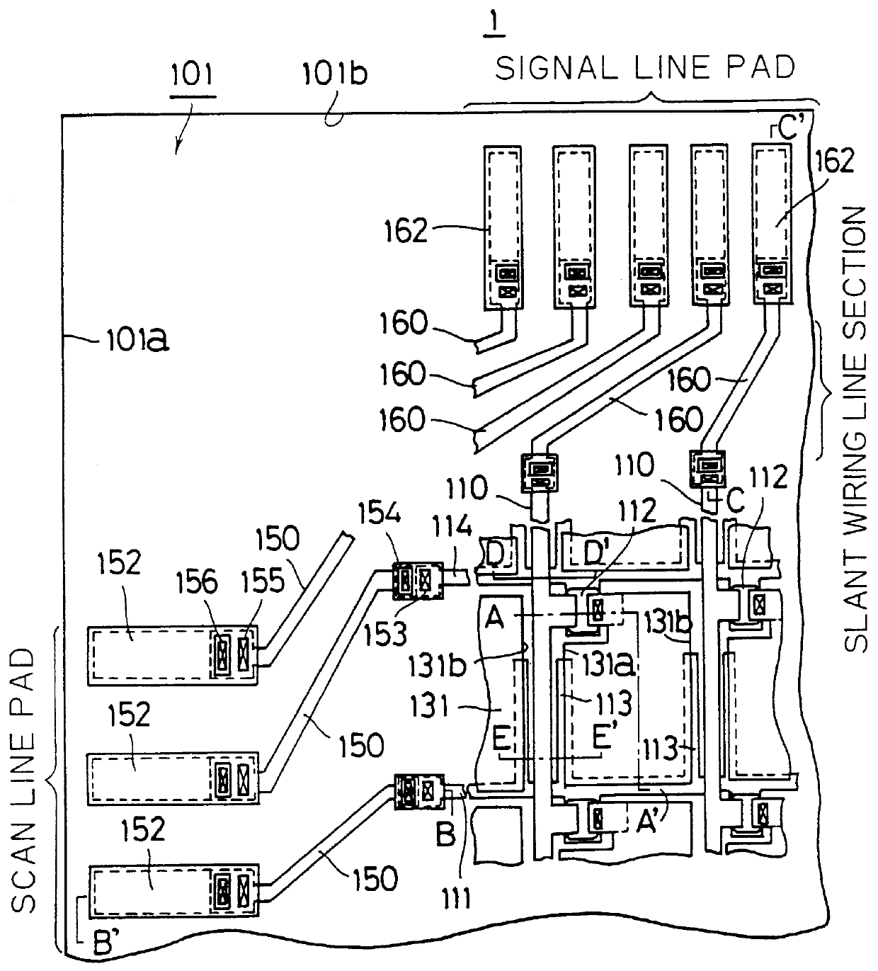
With the array substrate in accordance with the foregoing illustrative embodiment, the array substrate can be formed or manufactured by use of basically five masks. More specifically, the productivity can be improved with a decreased number of masks used while avoiding a decrease in the manufacturing yield thereof, as a result of locating the pixel electrodes at the uppermost position, and of employing a specific manufacturing method allowing several process steps to be done simultaneously which steps include: patterning the semiconductor coated films as well as the signal lines, source and drain electrodes at a time with the same mask pattern used therefor; forming the contact holes for interconnection of each source electrode and its associated pixel electrode; and forming the contact holes for exposure of contact nodes of signal lines and scanning line s.
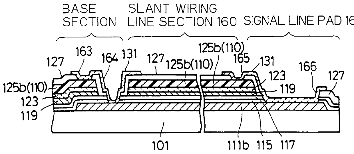
Further, each slant wiring line section of signal lines and scanning lines has a double-layered st...
second embodiment
Advantage of Second Embodiment
With the array substrate in accordance with the foregoing illustrative embodiment, the array substrate can be formed or manufactured by use of basically five masks. More specifically, the productivity can be improved with a decreased number of masks used while avoiding a decrease in the manufacturing yield thereof, as a result of locating the pixel electrodes at the uppermost position, and of employing a specific manufacturing method allowing several processes to be done at same step which steps include: patterning the semiconductor coated films as well as the signal lines, source and drain electrodes at a time using the same mask pattern; forming the contact holes for interconnection of each source electrode with its associated pixel electrode and the contact holes for exposure of contact nodes of signal lines and scanning line s.
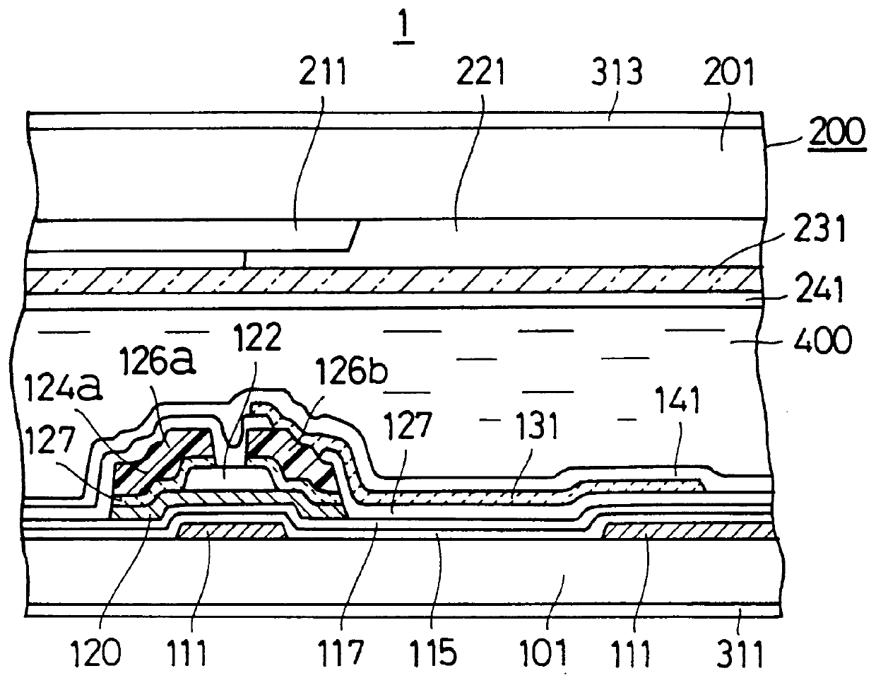
Further, in the manufacturing process steps mentioned above, it is possible to simultaneously form the pixel electrode (131)...
third embodiment
Advantage of Third Embodiment
With the array substrate in accordance with the foregoing illustrative embodiment, the array substrate can be formed or manufactured by use of basically five masks. More specifically, an optimized process can be provided for achievement of the conflicting requirements--namely, preventing a reduction in manufacturing yield by miniaturizing any possible step-like differences as caused in wiring lines, and improving the productivity with a decreased number of masks employed therein--as a result of locating the pixel electrodes at the uppermost position, and of employing a specific manufacturing method allowing several process steps to be done simultaneously which steps include: patterning the semiconductor coated films as well as the signal lines, source and drain electrodes at a time using the same mask pattern used therefor; forming the contact holes for interconnection of each source electrode with its associated pixel electrode and the contact holes for...
PUM
| Property | Measurement | Unit |
|---|---|---|
| thickness | aaaaa | aaaaa |
| thickness | aaaaa | aaaaa |
| thick | aaaaa | aaaaa |
Abstract
Description
Claims
Application Information