Chamber for reducing contamination during chemical vapor deposition
a technology of chemical vapor and chamber, which is applied in the direction of chemical vapor deposition coating, coating, metallic material coating process, etc., can solve the problems of increased manufacturing cost, reduced throughput and manufacturing cost, and low deposition rate, so as to reduce the amount of byproduct buildup
- Summary
- Abstract
- Description
- Claims
- Application Information
AI Technical Summary
Benefits of technology
Problems solved by technology
Method used
Image

Examples
example 1
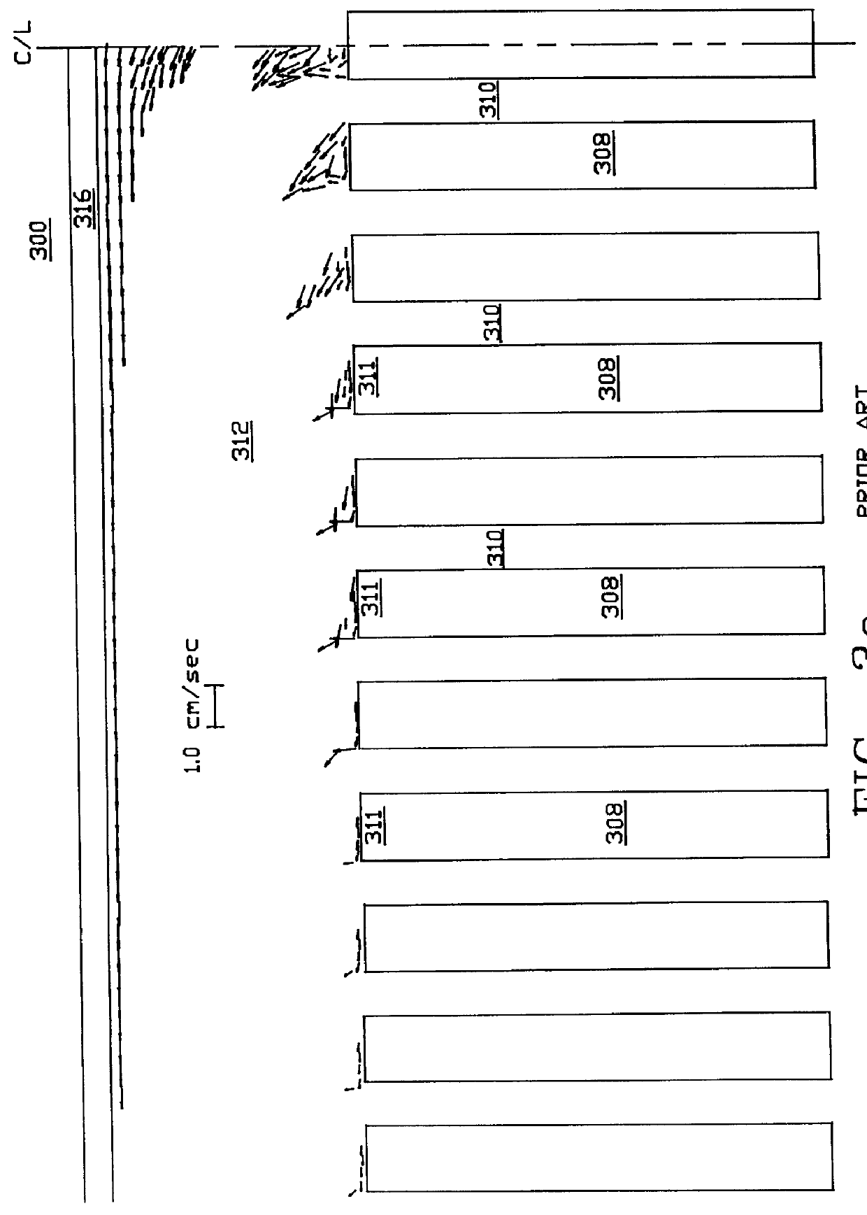
Deposition Rates Using Prior Art Gas Separator Plates
To quantify the effects of buildup of byproducts on the performance of dispersion plates, we performed a series of experiments in which we measured the film thickness of SiO.sub.2 (in .ANG.) deposited on a semiconductor substrate, through a dispersion head containing prior art gas separation plates. We deposited undoped silicate glass (USG) using a modified Quester 6000 prototype deposition system using tetraethylorthosiliane (TEOS) as the precursor. The dispersion head coolant (water) temperature was set to 8.degree. C. to 25.degree. C. The gap between the dispersion head and the wafer was set at 6 mm, with one dispersion head set at 5 mm, and the wafer temperature was set at 500.degree. C. This configuration resulted in a temperature at the center of the dispersion head of 100.degree. C., and an average temperature of 70.degree. C. The TEOS flow rate was 30 standard liters / min, and the deposition time was 300 sec. The ozone conc...
example 2
Deposition Rates Using Prior Art Gas Separator Plates
To determine whether gas separator plates of the invention decreased the sensitivity of deposition rate due to total film deposited, we performed a series of experiments as described above in Example 1 except for replacing the gas separator plates of one half of dispersion head B with the rounded edge design shown in FIGS. 4a-4d.
The results are shown in FIG. 8, which is a graph of film deposition rate as a function of the total deposited film since the last cleaning of byproducts from the dispersion head. The half of the dispersion head with prior art gas separation plates are shown by diamonds ("standard"), and the half of the dispersion with gas separation plates of the invention are shown as filled squares ("radiused").
The prior art plates showed similar sensitivity of deposition rate on the total film deposited by the dispersion head. The slope of the relationship is of similar magnitude and error as for the previous experimen...
PUM
| Property | Measurement | Unit |
|---|---|---|
| diameters | aaaaa | aaaaa |
| diameters | aaaaa | aaaaa |
| diameters | aaaaa | aaaaa |
Abstract
Description
Claims
Application Information
 - R&D
- Intellectual Property
- Life Sciences
- Materials
- Tech Scout
- Unparalleled Data Quality
- Higher Quality Content
- 60% Fewer Hallucinations
Browse by: Latest US Patents, China's latest patents, Technical Efficacy Thesaurus, Application Domain, Technology Topic, Popular Technical Reports.
© 2025 PatSnap. All rights reserved.Legal|Privacy policy|Modern Slavery Act Transparency Statement|Sitemap|About US| Contact US: help@patsnap.com