Wiring layer and method of forming the wiring layer

a wiring layer and wiring layer technology, applied in the field of wiring layer and method of wiring layer, can solve the problems of low melting point, increased display size, signal delay and heat generation

Inactive Publication Date: 2000-07-18
AU OPTRONICS CORP
View PDF5 Cites 8 Cited by
  • Summary
  • Abstract
  • Description
  • Claims
  • Application Information

AI Technical Summary

Problems solved by technology

If the electric resistance is high, various problems such as signal delay and heat generation will arise when the liquid crystal display is increased in its size.
However, pure aluminum has the disadvantage that the melting point is low and it will easily give rise to defects, called hillocks or whiskers, by a thermal process using chemical vapor disposition (CVD) after formation of a wiring film.
Therefore, if formation of these insulating layers is not sufficient, a problem such as an interlayer short circuit will arise between an electrode which is formed on an overlying layer and an electrode which is formed on an underlying layer.
For this reason, an occurrence of the hillock and the like will become an extremely large problem in the process of fabricating liquid crystal displays.
However, these high-melting point metals are wiring mat

Method used


Image

  • Wiring layer and method of forming the wiring layer
  • Wiring layer and method of forming the wiring layer
  • Wiring layer and method of forming the wiring layer

Examples


Embodiment Construction

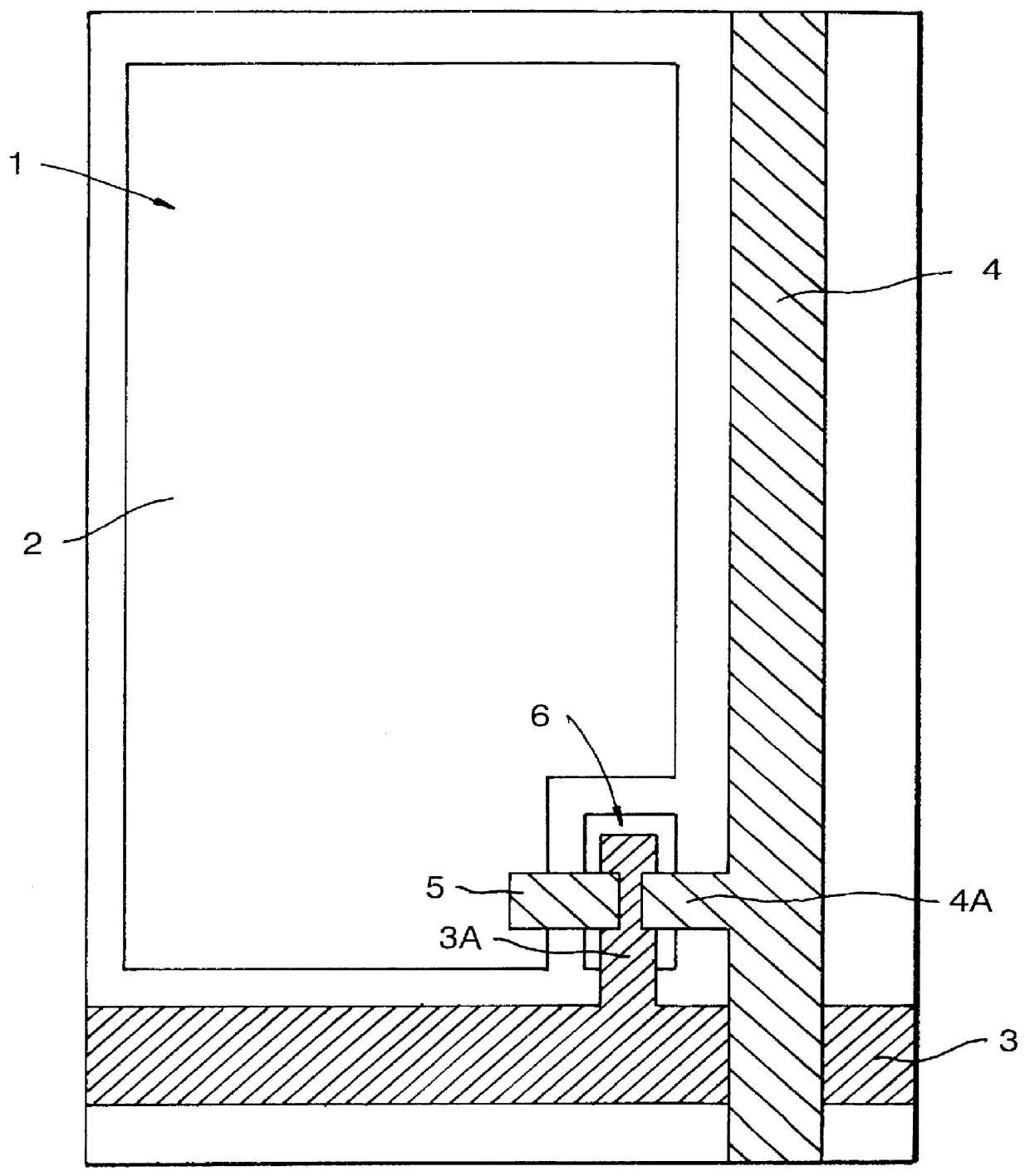
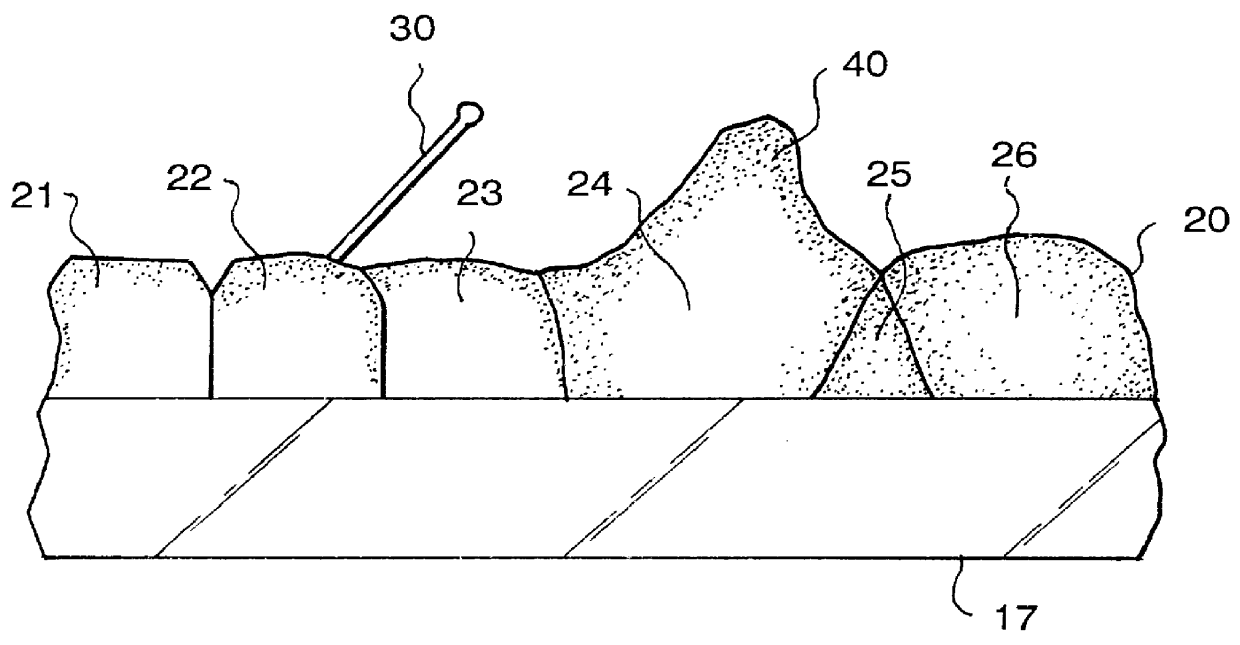
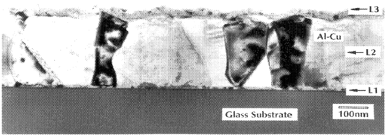
In the present invention, a stacked structure with a plurality of stacked metal layers having substantially the same composition is formed by using aluminum (Al) as a base and adding Cu and the like as additive elements, to satisfy aforementioned characteristics. In general, if an additive element is added to aluminum (Al), the electric resistance tends to increase. Particularly when an additional element is fused into an aluminum (Al) base, this tendency becomes intense. Therefore, investigations were made in quest of elements which can improve a resistance to thermal stress by a very small quantity of addition and prevent an occurrence of defects such as hillocks and the like, and at the same time, attempts were made to form a stacked structure by the same materials, the same processing room, and continuous discharging and to form a wiring structure with a strong resistance to stress migration and low electric resistance.

The principles of the present invention are derived from the...


PUM


Abstract

The present invention is directed to a wiring layer which has high thermal stability and a better stress migration resistance characteristic as an electrode wiring material that is used in a liquid crystal display and where there is no defect such as a hillock and the like and the electric resistance is considerably low. More specifically, the present invention is directed to a wiring layer which comprises at least two layers formed on a substrate. The two layers include: a first layer which has substantially aluminum for its main component and a second layer formed on the first layer which has substantially the same component as the first layer. Also, the second layer is higher in electric resistance than the first layer and has an amorphous phase for its main phase. The second layer may also include microcrystals which have a crystal particle diameter D2 smaller than a crystal particle diameter D1 of the first layer.

Description

1. Technical FieldThe present invention relates to an electrode structure which has low resistance and high thermal stability as an electrode wiring material for liquid crystal displays and where an occurrence of stress migrations such as hillocks and whiskers is completely suppressed, and also relates to a method of forming the electrode structure.2. Prior ArtPure metal, such as Cu, Al, Mo, Ta, and W, or alloy material, such as Al--Cu, Al--Cu--Si, Al--Pd, has hitherto been employed in the low-resistance electrode wiring material that is employed in semiconductor devices. On the other hand, particularly in the electrode material for liquid crystal displays which have been attracting attention as flat panel displays, there have recently been required better characteristics than before, such as large area wiring for large screens, high integrated wiring for high fineness, and array formation which is the film formation onto a glass substrate. In FIG. 1 there is shown a schematic diagr...

Claims


Application Information

Patent Timeline
IPC IPC(8): H01L21/70H01L21/768H01L21/28H01L21/3205H01L23/52
CPCH01L21/76838
Inventor TAKATSUJI, HIROSHITSUJI, SATOSHIKITAHARA, HIROAKI
Owner AU OPTRONICS CORP
Why Eureka
Try Eureka