Method of and apparatus for automatic high-speed optical inspection of semi-conductor structures and the like through fluorescent photoresist inspection

a technology of fluorescent photoresist and automatic high-speed optical inspection, which is applied in the direction of optical investigation of flaws/contamination, semiconductor/solid-state device testing/measurement, instruments, etc., to achieve the effect of high speed

Inactive Publication Date: 2000-07-18
BELTRONICS
View PDF2 Cites 70 Cited by
  • Summary
  • Abstract
  • Description
  • Claims
  • Application Information

AI Technical Summary

Benefits of technology

It is accordingly an object of the present invention to provide a new and improved method of and apparatus for enabling the high speed optical scanning inspection of multi-layer wafers, chips and other semi-conductors and similar devices, that shall not be subject to the prior art limitations ab...

Problems solved by technology

The use of fluorescence in inspection systems for other purposes has also been taught, as, for example, fluorescing epoxy circuit boards to enable ignoring grainy metallic co...

Method used


Image

  • Method of and apparatus for automatic high-speed optical inspection of semi-conductor structures and the like through fluorescent photoresist inspection
  • Method of and apparatus for automatic high-speed optical inspection of semi-conductor structures and the like through fluorescent photoresist inspection
  • Method of and apparatus for automatic high-speed optical inspection of semi-conductor structures and the like through fluorescent photoresist inspection

Examples


Embodiment Construction

Before preceding to describe preferred apparatus for implementing the novel inspection method or technique underlying the present invention, it is believed useful and important first to review how semi-conductor structures are fabricated, and the possible defects in photoresist-conductor pattern etching on developing that it is important to detect by automatic or machine optical inspection.

Introduction

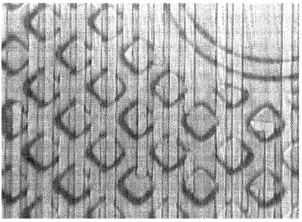
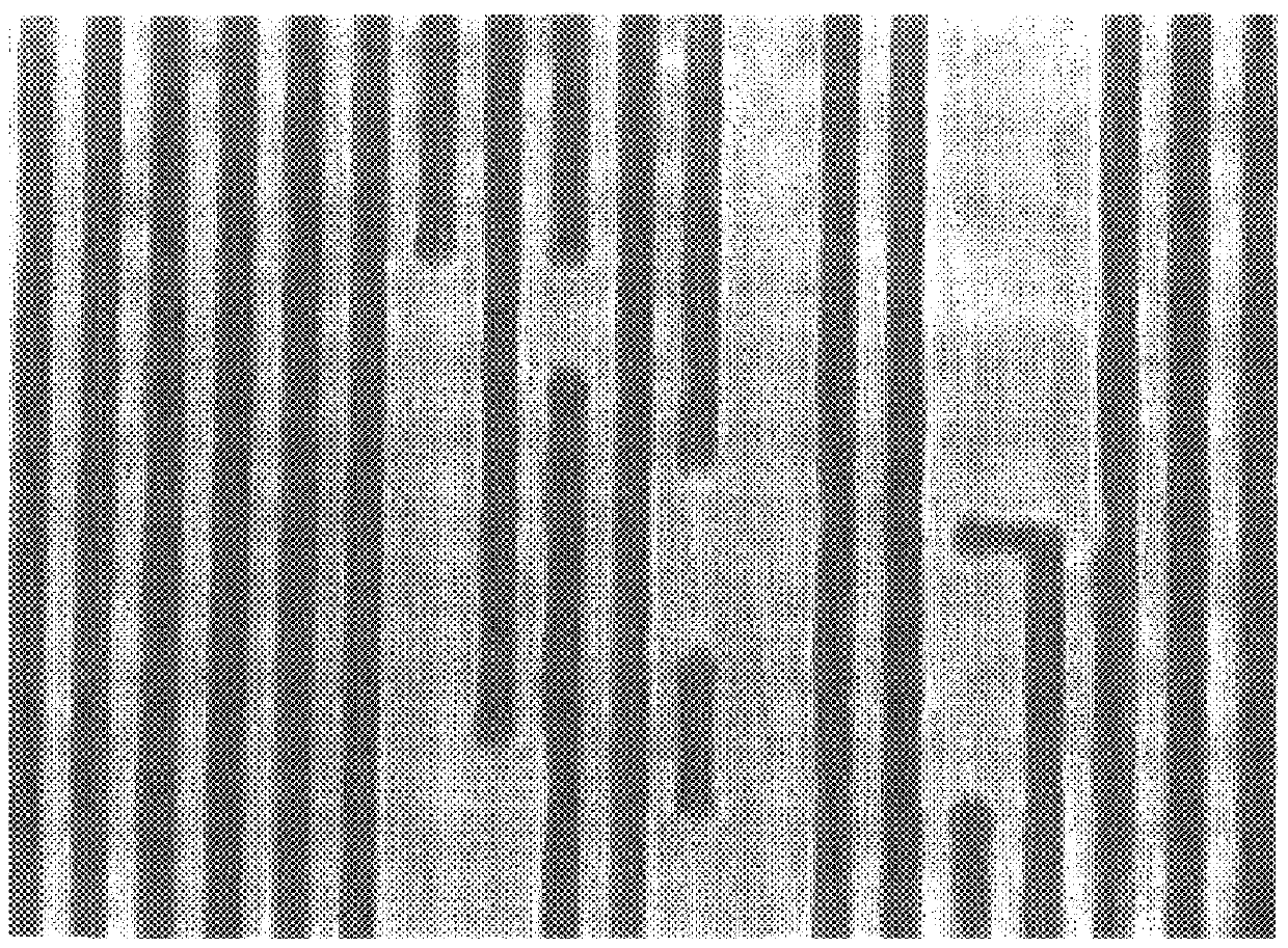
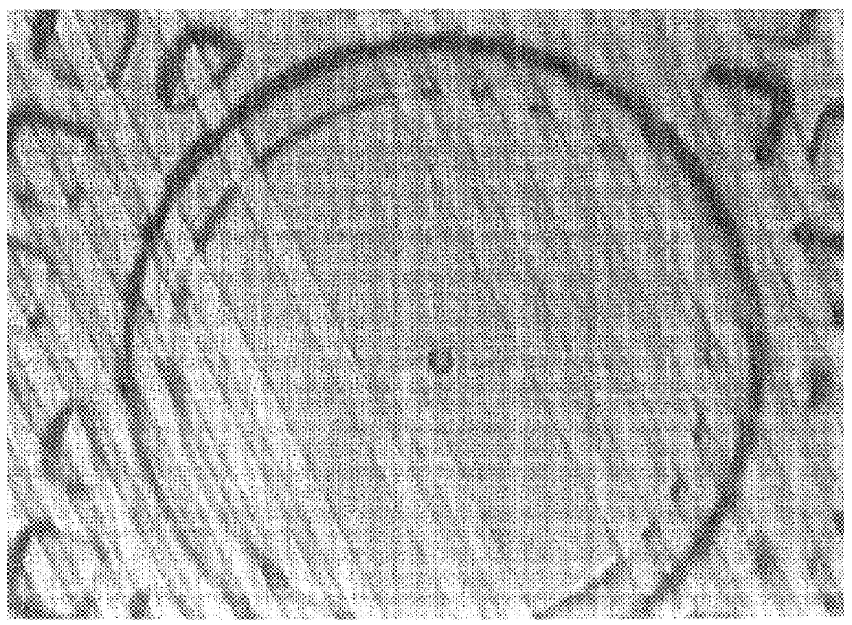
As before explained, semiconductor wafers and the like consist of one or more layers of conducting (metal) material. Fabrication of each layer requires the deposition of photoresist to define where the circuit structures are to be placed.

Fluorescence, as also previously explained, can be used to inspect the photoresist pattern. When the photoresist is deposited on metal, this invention enables the resist pattern to be inspected before etching the metal beneath. One can repair a defect in the resist stage; but it is much more difficult, perhaps impossible, to do so after etching.

Both po...


PUM


Abstract

Semiconductor wafers, circuit boards and similar multi-layer structures are optically inspected at high speeds with the aid of preferably a pair of oppositely and inclinedly directed laser beams at inclined angles to the vertical and the wafer surface to cause fluorescence by a photoresist layer carrying conductor patterns, defects in which are to be inspected, and using preferably a time-delay-integration CCD imaging camera for recording a fluorescent resist surface image accentuating the non-fluorescing conductor pattern thereupon, while masking all light from layers therebelow.

Description

The present invention relates to the optical inspection of semi-conductor structures and the like, such as multi-layer wafers, chips, circuit boards, etc., being more specifically, though not exclusively, concerned with high speed inspection for defects or artifacts and the like, and to the employment therein of selective layer fluorescence as an aid to preferential discriminative or selective imaging of predetermined surfaces or layers or parts of such structures.The use of a laser-beam-excited fluorescing top dielectric layer of a multi-layered semi-conductor wafer or chip or the like for the purpose of shadowing conductor patterns deposited on controlled flat surfaces thereof, and thereby masking layers therebelow, is described in U.S. Pat. No. 5,278,012 to Yamanaka et al; and improvements thereupon for enabling the use of such techniques with rough or randomly bumpy layers or surfaces and protruding angle conductors is accomplished by the techniques described in my co-pending U....

Claims


Application Information

Patent Timeline
IPC IPC(8): G01N21/88G01N21/956H01L21/66
CPCG01N21/956H01L22/00
Inventor BISHOP, ROBERT
Owner BELTRONICS
Why Eureka
Try Eureka