Dishing avoidance in wide soft metal wires

a soft metal wire, wide technology, applied in the direction of conductive pattern formation, total factory control, instruments, etc., can solve the problems of increasing the resistance of a tiled wire by about 12%, reducing the correctness of design and yield, and increasing the turn-around tim

Inactive Publication Date: 2000-08-01
IBM CORP
View PDF1 Cites 14 Cited by
  • Summary
  • Abstract
  • Description
  • Claims
  • Application Information

AI Technical Summary

Problems solved by technology

However, as already mentioned above, these methods involve additional process steps leading to increased turn-around-times and decreased correctness of the design and yield.
However, this proposal has the disadvantage that the resistance of a tiled wire increases by about 12% due to a loss of metal where the negative fill shapes are introduced.
Furthermore, the determination of areas to be tiled and the introduction of the unit cells into the layout data is very complicated and increases the turn-around-time in a high degree.
Since the number of shapes increases by about the factor 1000, handling the resulting data is also very complicated (e.g., DRC checking).
An alternate tiling pattern could reduce the number of shapes but not significantly and unfortunately only in conjunction with higher wiring resistance.
In addition to that, tiling is applied after via insertion, hence it cannot be guaranteed that groundrules for DRC can be met.

Method used


Image

  • Dishing avoidance in wide soft metal wires
  • Dishing avoidance in wide soft metal wires

Examples


Embodiment Construction

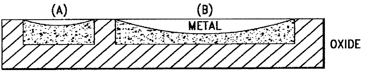
As can be taken from FIG. 1, dishing occurs within smaller lines as well as within wide lines. Within smaller lines (A) this effect can be neglected up to a certain degree, whereas for wider lines (B) dishing shows a big impact onto the metal's resistance and on the manufacturability.

The present invention describes the technique of splitting up wide metal areas into metal stripes from the very beginning of the design, i.e., the step of splitting up the metal areas is already included into the physical design. Thus, splitting of wide lines forms part of the steps of building and placing of the functional elements as well as their wiring within the metal layers.

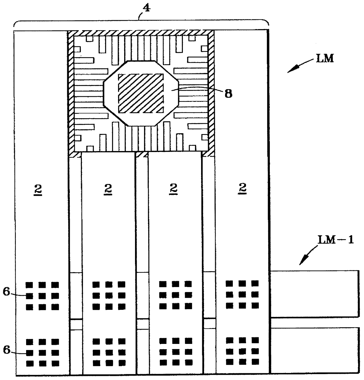
In the following it is described how wires are split up, how the interconnection between distinct metal layers is handled, what is needed to connect to tiled Controlled Collapse Chip Connections (C4s) and how a power grid is designed using very wide--but split up--wires to keep the voltage drop across the grid as low as with no...


PUM

PropertyMeasurementUnit
widthaaaaaaaaaa
semiconductoraaaaaaaaaa
geometric shapesaaaaaaaaaa

Abstract

A method of manufacturing semiconductor circuits or electronic packages is provided. The step of splitting up wide metal areas into metal stripes is included into the physical design step of such devices. This method does not increase the data complexity significantly and guarantees correctness of the design. Furthermore, the method allows to solve the dishing problem that is inherent to copper wiring technologies.

Description

The present invention generally relates to the art of microelectronic circuit fabrication, and more specifically to the physical design of a microelectronic integrated circuit. Still more specifically, it relates to the avoidance of dishing of weak metal like copper during the process of planarization by chemical-mechanical polishing (CMP).Semiconductor integrated circuits and printed circuit electronic packages are generally structures consisting of several layers of conducting, insulating and other materials that are structured in the horizontal dimension by fabrication processes that transfer patterns defined in physical designs or layouts. A layout consists of a set of planar geometric shapes in several layers. These physical designs or layouts are typically represented as computer data consisting of two dimensional shapes in a hierarchical data structure that exploit the repetitive structure usually found in such circuits and packages. The design files are then converted into p...

Claims


Application Information

Patent Timeline
Patent Type & Authority Patents(United States)
IPC IPC(8): H01L21/70H01L21/768
CPCG06F17/5068H01L21/7684G06F2217/12Y10T29/49121Y10T29/49155Y10T29/49165G06F30/39G06F2119/18Y02P90/02
Inventor ENGLISH, GEORGEKEINERT, JOACHIMRETTIG, OLIVER
Owner IBM CORP
Why Eureka
Try Eureka