LDD structure for ESD protection and method of fabrication

a technology of esd protection and fabrication method, which is applied in the direction of semiconductor devices, instruments, optical means, etc., can solve the problems of system failure, failure of the entire esd protection device, and adverse effects on the operation of the circuit,

Inactive Publication Date: 2000-08-08
SEMICON COMPONENTS IND LLC
View PDF20 Cites 49 Cited by
  • Summary
  • Abstract
  • Description
  • Claims
  • Application Information

AI Technical Summary

Problems solved by technology

When that occurs, operation of the circuit can be adversely affected, including the possibility of system failure.
Failure to do so will result in the first of the transistors in the set to turn on to support the entire transient load.
That generally causes failure of that transistor unit as well as the entire ESD protection device.
Ballast resistance is required in these devices as a means to alleviate problems of non-simultaneous turn-on; however, the ballast that is often required can lead to unacceptable increases in transistor set size.
Variations occurring during processing of the prior ballasted ESD devices further tend to yield unreliable ESD protection, particularly where vertical pathways and field oxides were relied upon to provide the resistance.
While tremendous effort is made to make the fabrication of semiconductor devices as accurate as possible, there will remain vagaries in active device characteristics from one production run to another and even within production runs.
The field oxide is dopant deficient such that it is a poor conductor with respect to the active areas of the fabricated semiconductor product.
However, prior attempts at improving ballast resistances in ESD protection devices have come at the expense of modifying the silicide layer and thereby impairing optimization of gate operation.
However, in standard fabrication processes of the type described, there are steps taken to enhance transistor action that adversely affect ESDP capability.
These contrasting goals...

Method used


Image

  • LDD structure for ESD protection and method of fabrication
  • LDD structure for ESD protection and method of fabrication
  • LDD structure for ESD protection and method of fabrication

Examples


Embodiment Construction

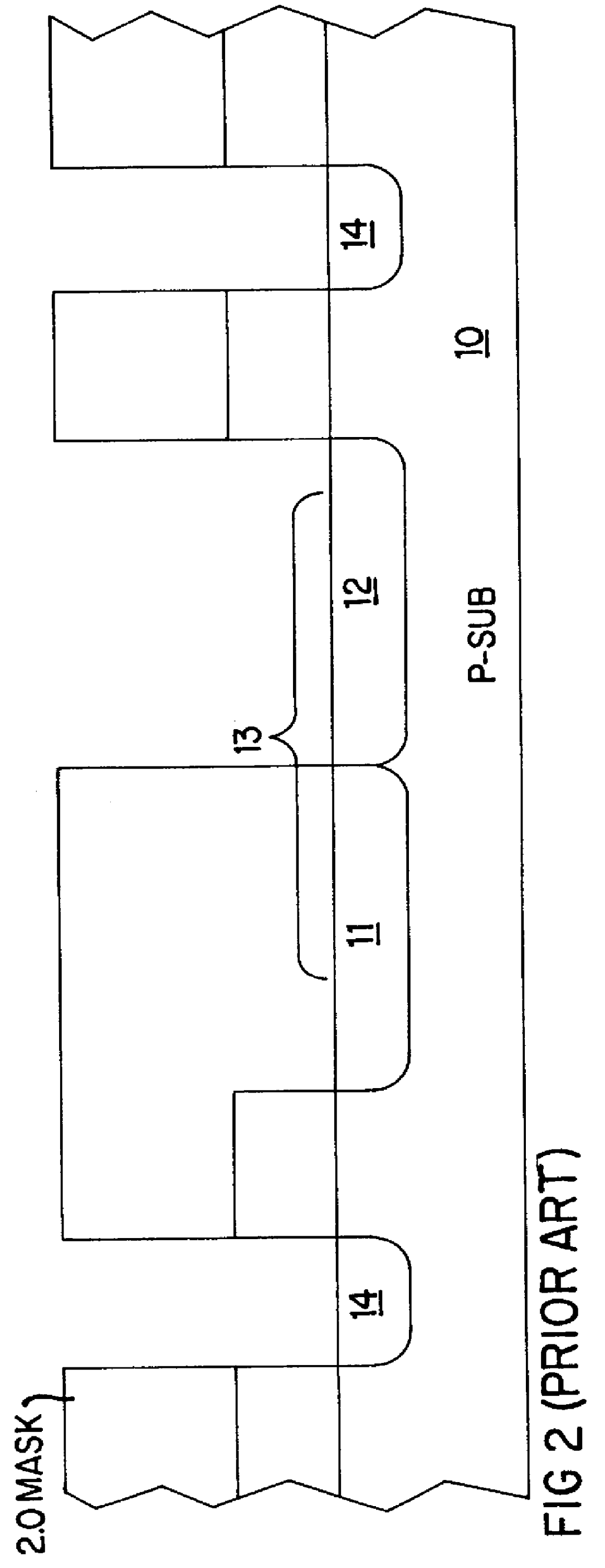
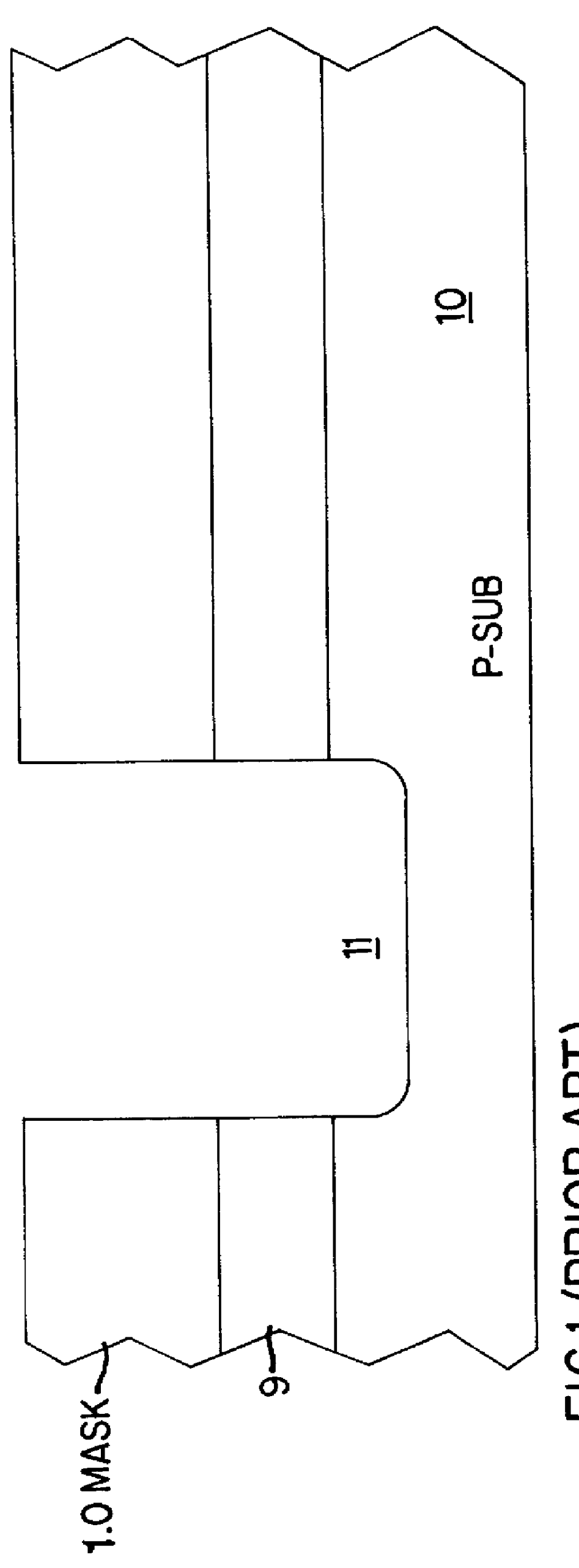
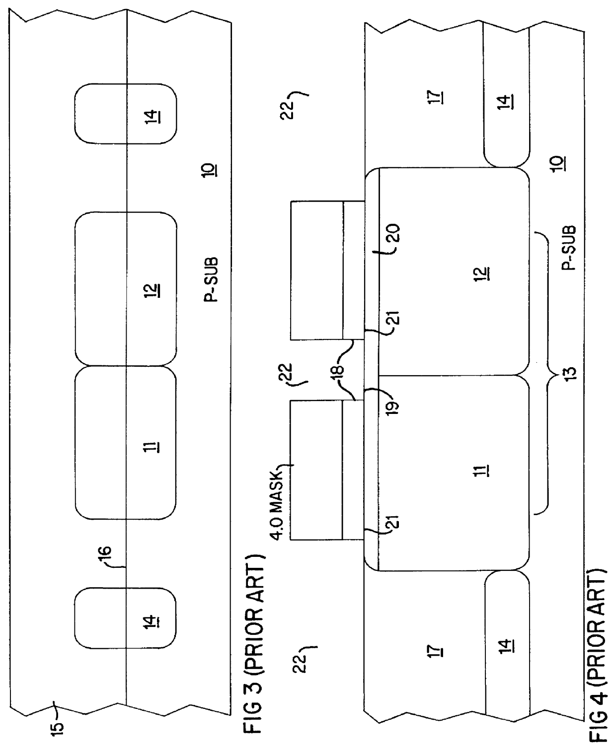
A method of fabricating a new ESD protection transistor of the present invention is described in conjunction with a series of fabrication steps shown in FIGS. 1-12. The fabrication process used to form one or more ESD protection transistors has been integrated into CMOS fabrication steps previously noted, without adding any new steps. New CMOS mask structures are shown in FIGS. 9-12. The overall CMOS transistor structure mask sequence is the sequence summarized in the Summary of the Invention. While the present discussion relates to the formation of an NMOS transistor with an N type LDD resistive region, it is to be understood that the LDD region introduced may also be a P type LDD region, forming a PMOS transistor. However, in most instances, NMOS transistors are commonly used as buffers against the effects on input / output nodes of electrostatic discharges.

Prior to the fabrication sequences used to form the transistor structure of the present invention, an initial oxide layer 9 is ...


PUM


Abstract

An ESD protection device including a transistor structure with resistive regions located within active areas thereof. The transistor structure is formed of one or more MOS transistors, preferably N-type MOS transistors. The drain regions of the transistors are modified to reduce the conductivity of those resistive regions by preventing high carrier concentration implants in one or more sections of the drain regions. This is achieved by modifying an N LDD mask and the steps related thereto, as well as a silicide exclusion mask and the steps related thereto. The modifications result in the omission of N LDD dopant from the area immediately adjacent to the underlying channel. In addition, portions of a spacer oxide remain over the drain region to be formed. Subsequent implant and siliciding steps are effectively blocked by the spacer oxide that remains, leaving a low-density drain (LDD) charge carrier concentration in those regions, except where omitted. The resistivity of those resistive LDD regions is greater than the resistivity of the adjacent portions of the drain region. The result is more uniform turn-on of ESD transistor fingers in a protection device set without the need to add valuable layout space and without increased processing steps.

Description

1. Field of the InventionThe present invention relates to Electrostatic Discharge Protection (ESDP) devices. In particular, the present invention relates to Metal-Oxide-Silicon (MOS) transistors used to provide ESDP, including, but not limited to, N-type MOS transistors. More particularly, the present invention relates to the introduction of a tailored low-density drain (LDD) region of such MOS transistors to provide sufficient insulative characteristics without reliance upon standard field oxide isolation.2. Description of the Prior ArtThe fabrication of increasingly smaller integrated circuit (IC) devices has made the reliance upon effective smaller ESDP devices more important. It is well known that transient voltage surges, referred to as electrostatic discharges that may be thousands of volts, commonly occur at the input / output terminals of IC's. These terminals are electrically coupled to active circuit components including, but not limited to, bipolar and MOS transistors. It i...

Claims


Application Information

Patent Timeline
IPC IPC(8): H01L27/02H01L27/04
CPCH01L27/0266H01L27/0288H01L27/04
Inventor HULFACHOR, RONALD BRETTLEIBIGER, STEVENHARLEY-STEAD, MICHAELHAHN, DANIEL JAMES
Owner SEMICON COMPONENTS IND LLC
Why Eureka
Try Eureka