Means and method for mounting electronics

a technology of electronics and mounting methods, applied in the direction of casings/cabinets/drawers, electrical apparatus construction details, casings/cabinets/drawers details, etc., can solve the problems of high temperature, high thermal expansion resistance of the bedding, and high so as to achieve the effect of reducing the temperature of the bedding

Inactive Publication Date: 2000-08-22
TELEFON AB LM ERICSSON (PUBL)
View PDF24 Cites 33 Cited by
  • Summary
  • Abstract
  • Description
  • Claims
  • Application Information

AI Technical Summary

Benefits of technology

One object of the present invention is thus to provide a simple, low cost temperature compensating bedding in a printed board for a chip and to provide a simple, low cost method for manufacturing the temperature compensating bedding, the system comprising the chip on the temperature compensating bedding in the printed board being compact.
Yet another advantage is that the temperature compensating means may be placed anywhere in the printed board carrier where it is desirable to place the chip.

Problems solved by technology

Temperature variations arise, for example, as a current circulating in the circuits on the printed board causes heating of the circuits.
In general, the coefficient of thermal expansion for the chip and the bedding are different, whereby the chip and the bedding expand differently as the temperature varies, leading to great tensions being generated in the chip, subsequently liable to break.
A chip placed directly on a carrier, having a coefficient of thermal expansion different from the coefficient of thermal expansion of the chip, in a printed board cracks particularly easily during a cold start when the current is switched on through the chip and heat is dissipated within the chip.
Chips made from GaAs (Galium Arsenide), i.e. GaAs-chips, are very brittle and thereby considerably more sensitive to thermal expansions in the bedding than chips e.g. from silicon (Si-chips).
A drawback of the method described above is that the Cu--Mo--Cu-module and the Cu--Wo--Cu-module constitute fixed separate units which renders pattern etching below the chip more difficult.
A drawback of this method is that tungsten and molybdenum are expensive to use.

Method used


Image

  • Means and method for mounting electronics
  • Means and method for mounting electronics
  • Means and method for mounting electronics

Examples


Embodiment Construction

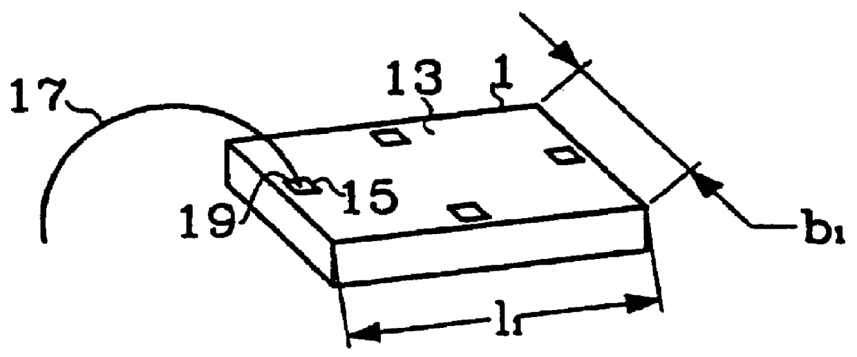
One problem addressed by the invention is providing a simple, low cost temperature compensating bedding for a chip on a printed board and providing a simple, low cost method for manufacturing the temperature compensating bedding.

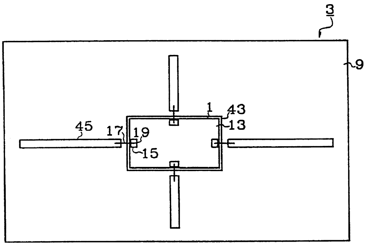
Another problem is providing a compact solution so that the chip on the temperature compensating bedding takes up little space on the printed board.

One object of the present invention is thus to provide a simple, low cost temperature compensating bedding in a printed board for a chip and to provide a simple, low cost method for manufacturing the temperature compensating bedding, the system comprising the chip on the temperature compensating bedding in the printed board being compact.

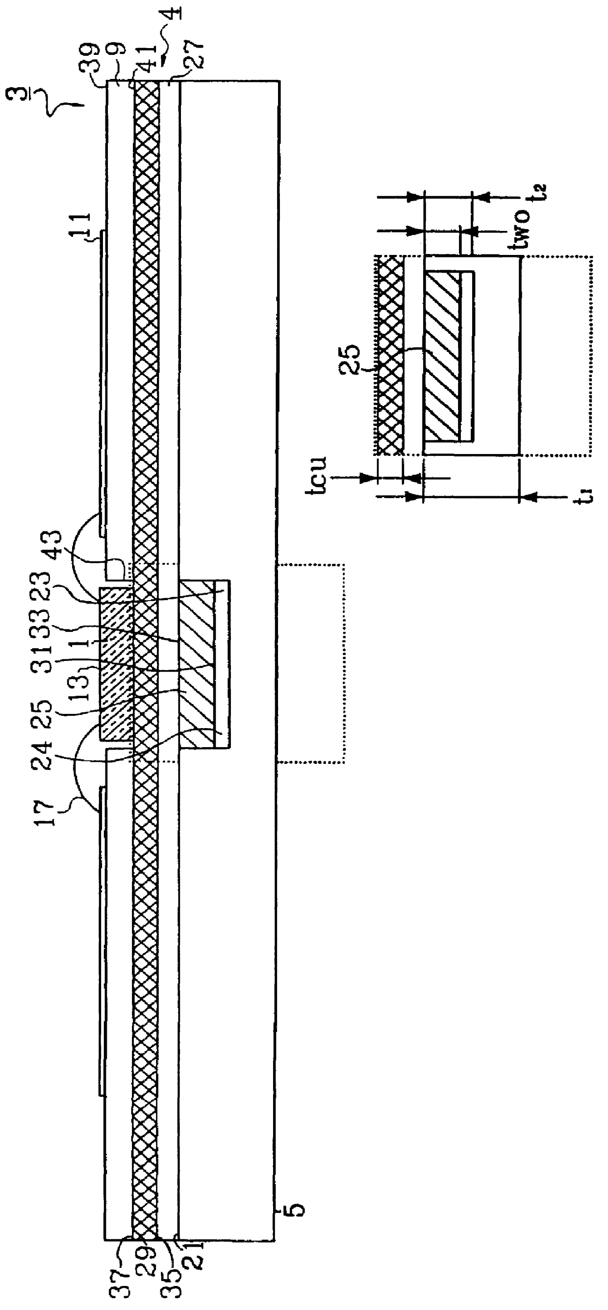
To accomplish this the present invention makes use of a temperature compensating means fully or partly inset in the carrier below the chip. The invention also uses e.g. a PFA-layer, both as isolating material and laminating material between the metal layers of the printed board.

M...


PUM


Abstract

The present invention relates to a method and device for making a temperature-compensated bedding for chips on printed boards, at which a temperature-compensated device is totally or partly recessed in a carrier in the printed board. The chips is placed over the temperature-compensated device. The temperature-compensated device includes a piece of metal recessed in the carrier under the chip. A layer of copper is fixed against the upper side of the carrier and the upper side of the metal piece. The thickness of the copper layer and the thickness of the metal piece are dimensioned so that the resulting coefficient of linear expansion at the upper side of the copper layer is equally big as or a bit bigger than the coefficient of linear expansion of the chip. The temperature-compensated device can as an alternative to the above include a module recessed in the carrier under the chip. A thin layer of dielectric is fixed against the carrier, so that the coefficient of linear expansion of the dielectric layer don't appreciable affect the resulting coefficient of linear expansion of the temperature-compensated device.

Description

The present invention relates to a device and a method for creating a temperature-compensating bedding for electronics on a printed board.STATE OF THE ARTA printed board is, according to the state of the art, a board made from several layers of suitable material. The bottom layer is, for example, called carrier and may consist of brass or FR4 epoxy glass. On the carrier, the remaining layers are arranged, such as for example one or more pattern layers, which are made from a suitable electrically conductive material, e.g. copper.Among others, three different known processes for manufacturing of printed boards are used: plating, contour milling and etching.Plating refers to the process of platting one layer of the printed board with a suitable electrical conducting substance, e.g. copper.Contour milling refers to the process of milling desired contours, e.g. recesses and contact pads, on the printed board. Electronic components, e.g. chips, can be connected to the contact pads on the ...

Claims


Application Information

Patent Timeline
Patent Type & Authority Patents(United States)
IPC IPC(8): H01L23/34H01L23/373H01L23/367H05K1/02H05K3/00H05K1/05H01L23/12H01L23/14
CPCH01L23/367H01L23/3735H05K1/0271H05K1/056H05K3/0061H05K2201/068H05K2201/10416H05K2201/10674H01L2224/16225H01L2224/48091H01L2224/48227H01L2224/49175H01L2924/00014H01L2224/05554H01L2924/00
Inventor BERGSTEDT, LEIF R.
Owner TELEFON AB LM ERICSSON (PUBL)
Why Eureka
Try Eureka