

Thin-film transistor array and method for manufacturing same
a transistor array and thin film technology, applied in the field of thin film transistor array and method for manufacturing same, can solve the problems of likely shortening, achieve the effects of reducing production loss, improving yield and product quality, and increasing parasitic capacitan
- Summary
- Abstract
- Description
- Claims
- Application Information
AI Technical Summary
Benefits of technology
Problems solved by technology
Method used
Image

Examples
embodiment 1
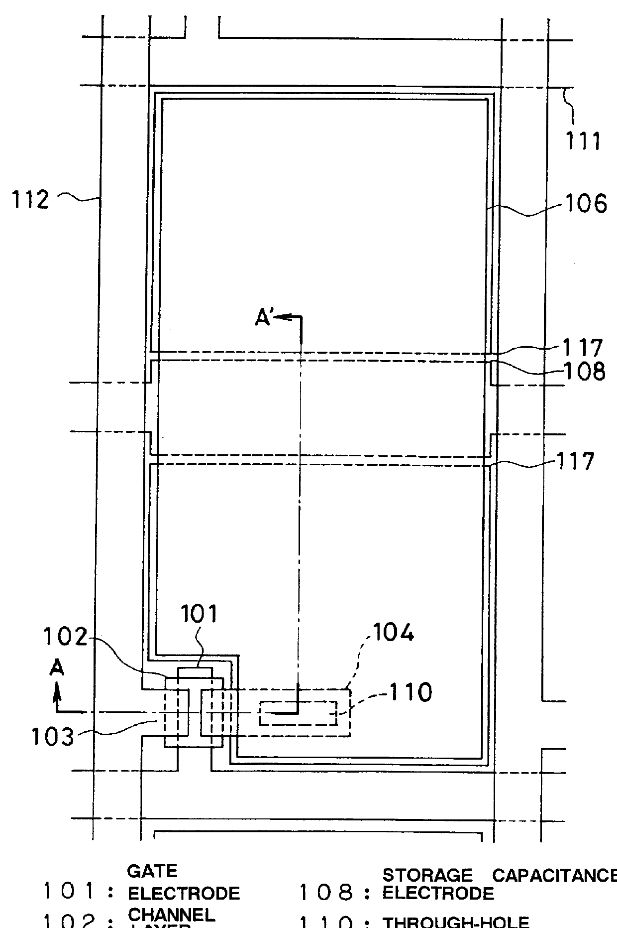
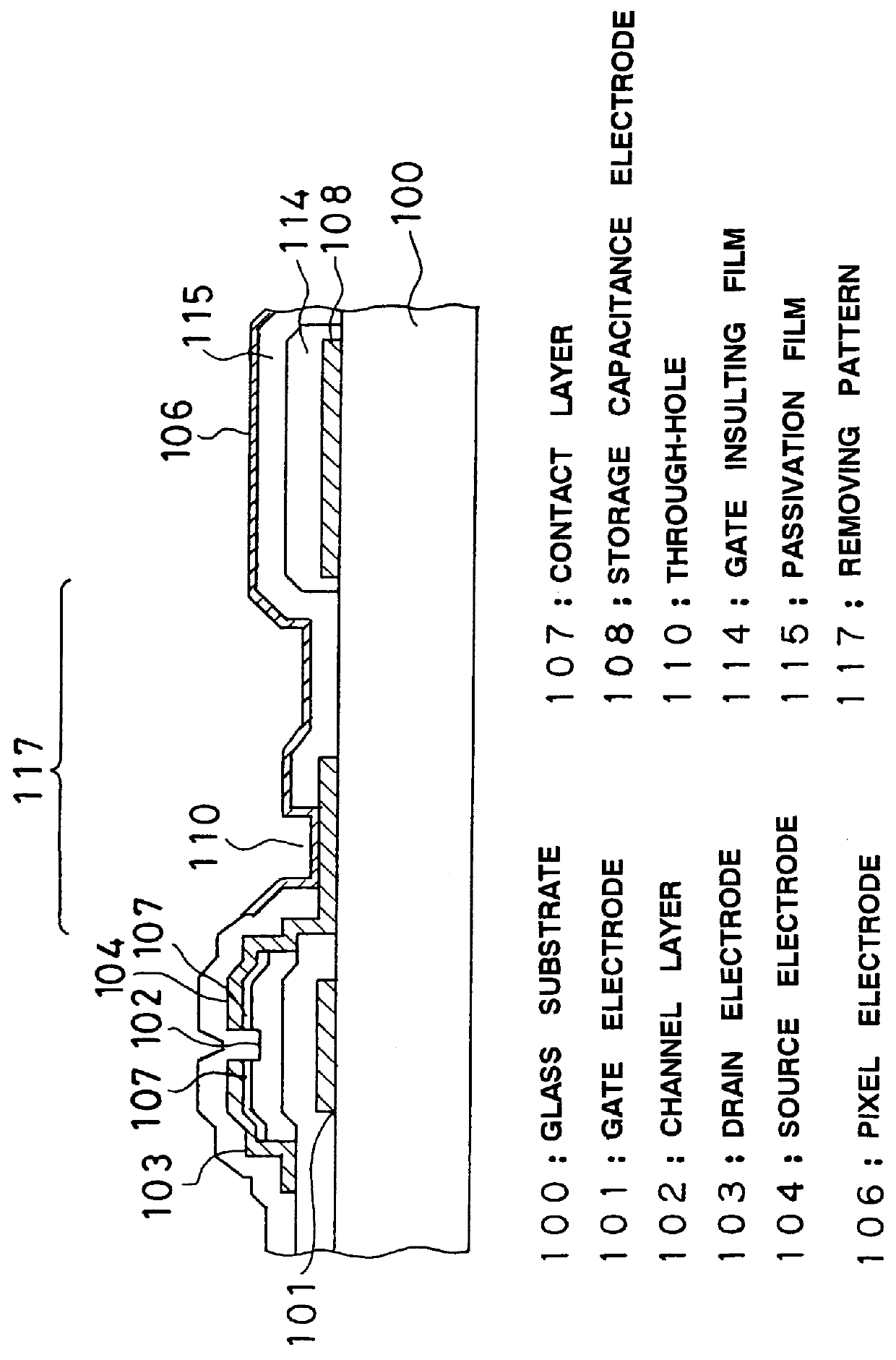
FIG. 1 and 2 show a plan view illustrating a first embodiment of a thin-film transistor array of the present invention and a cross-sectional view taken along line A-A' of FIG. 1, respectively.
Referring to FIGS. 1 and 2, the structure of the first embodiment of the present invention is explained.
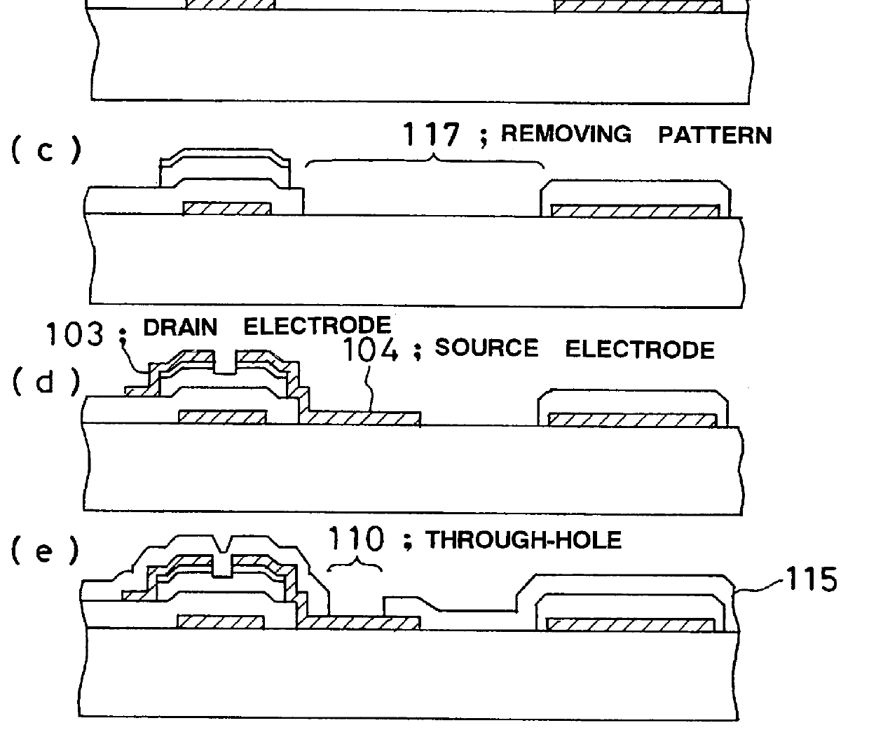
In the first embodiment of the present invention, there exist two layers, namely a gate insulating film 114 and a passivation film 115 as upper layers of the gate electrode 101 and the gate bus line 111. However, the insulating film for the pixel electrode disposed below the pixel electrode 106 is made up only of the passivation film 115. Namely 117 termed as "removing pattern" designates an area where the gate insulating film 114 has been removed.
The passivation film 115, as an insulating film, is interposed between a drain bus line 112 and the pixel electrode 106. Namely, the drain bus line 112 is disposed below the passivation film 115, whereas the pixel electrode 106 is above the passivat...
second embodiment
the present invention is characterized in that the storage capacitance electrode 108 is used simultaneously as the gate bus line 101 and is otherwise the same as the above-described first embodiment.
In the second embodiment of the present invention, the insulating film for the pixel electrode, extending over a partial area 117 lying below the pixel electrode 106, is constituted solely by the passivation film 115, as in the first embodiment, so that residual a-Si produced due to patterning defects during the island forming step can be removed simultaneously. This reduces occurrences of defects of semi-bright spots, otherwise caused by increased parasitic capacitance between the drain bus line 112 and the pixel electrode 106 on interconnection to the drain bus line 112 to suppress the reject ratio to improve the production yield.
Moreover, since there is the insulating passivation film 115 as a boundary separating film between the drain bus line 112 and the end of the pixel electrode 1...
third embodiment
the present invention is characterized in that, in removing the gate insulating film 114 lying below the pixel electrode of each unit pixel, there is formed a removing pattern 117 in the form of a slot a few micrometers in width along the drain bus line 112 and is otherwise the same as the above-described first embodiment.
For illustrating the operation and result of the third embodiment of the present invention, FIG. 10 shows a plan view illustrating the state of residual a-Si produced on a pixel. FIG. 11 shows a cross-sectional view taken along line E-E' of FIG. 10.
With the third embodiment of the present invention, the gate insulating film 114 of a partial area 117 lying below the pixel electrode is removed in the contact step in the form of slits several micrometers in width along the drain bus line 112 for simultaneously removing residual a-Si 116 produced due to patterning defects during the island step. This reduces occurrences of point defects of semi-bright spots otherwise p...
PUM
| Property | Measurement | Unit |
|---|---|---|
| transparent | aaaaa | aaaaa |
| area | aaaaa | aaaaa |
| storage capacitance | aaaaa | aaaaa |
Abstract
Description
Claims
Application Information