Method for high temperature etching of patterned layers using an organic mask stack

a high-temperature etching and organic masking technology, applied in the field of patterned etching, can solve the problems of dispersion of patterns and removal of residual silicon dioxide hard masking materials

Inactive Publication Date: 2000-11-07
APPLIED MATERIALS INC
View PDF29 Cites 187 Cited by
  • Summary
  • Abstract
  • Description
  • Claims
  • Application Information

AI Technical Summary

Problems solved by technology

This could lead to distortion of the pattern which is transferred to conductive layer 106.
At this point, the problem is the removal of the residual silicon dioxide hard masking material and the removal of residue deposits of the silicon dioxide masking material from adjacent surfaces.

Method used


Image

  • Method for high temperature etching of patterned layers using an organic mask stack
  • Method for high temperature etching of patterned layers using an organic mask stack
  • Method for high temperature etching of patterned layers using an organic mask stack

Examples


Embodiment Construction

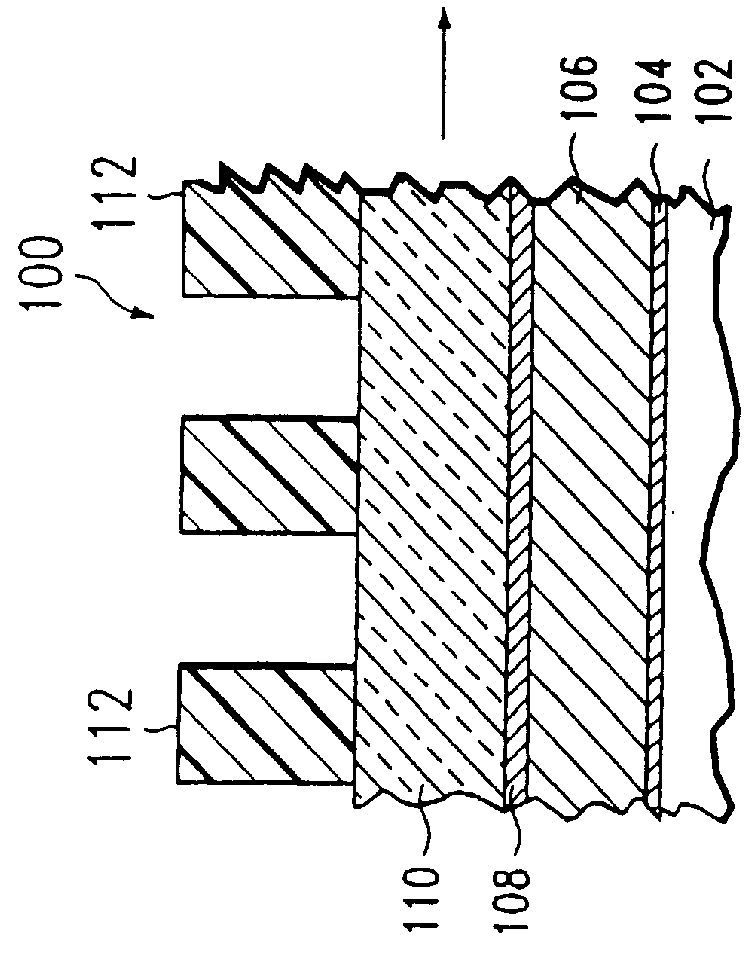
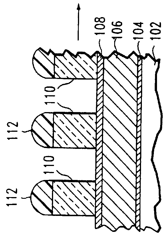
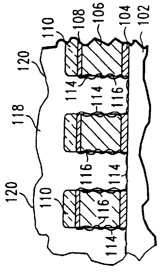
FIGS. 2A-2G illustrate the first preferred embodiment etch stack of the present invention as it progresses through the method steps of the present invention. FIG. 2A shows the complete etch stack 210, including: Substrate 212, which was a dielectric layer of silicon dioxide approximately 1,000 .ANG. thick overlying a silicon wafer surface (not shown). A barrier layer 214, of tantalum nitride approximately 500 .ANG. thick was deposited over substrate 212. A layer 216 of copper approximately 8,000 .ANG. thick was deposited over barrier layer 214. A layer 218 of tantalum nitride about 500 .ANG. thick, which served as a barrier layer, was deposited over copper layer 216. A layer 220 of a high-temperature organic-based pattern masking material comprising .alpha.-FC was deposited over tantalum nitride layer 218 using a high density plasma CVD technique, to produce a layer approximately 8,000 .ANG. thick. A silicon dioxide pattern masking layer 222, approximately 1,000 .ANG. thick, which s...


PUM

PropertyMeasurementUnit
feature sizesaaaaaaaaaa
temperaturesaaaaaaaaaa

Abstract

The present disclosure pertains to a method of patterning a semiconductor device feature which provides for the easy removal of any residual masking layer which remains after completion of a pattern etching process. The method provides for a multi-layered masking structure which includes a layer of high-temperature organic-based masking material overlaid by either a layer of a high-temperature inorganic masking material which can be patterned to provide an inorganic hard mask, or by a layer of high-temperature imageable organic masking material which can be patterned to provide an organic hard mask. The hard masking material is used to transfer a pattern to the high-temperature organic-based masking material, and then the hard masking material is removed. The high-temperature organic-based masking material is used to transfer the pattern to an underlying semiconductor device feature.

Description

1. Field of the InventionThe present invention pertains to a method for patterned etching of materials such as copper, platinum, iridium, ruthenium, tungsten, and barium strontium titanate, which generally requires higher temperature stability of the stack of masking materials used during the patterned etching. In addition to high temperature functionality, the stack of masking materials is designed to minimize the amount of masking material residue and sidewall deposits remaining on feature surfaces after etching.2. Brief Description of the Background ArtIn the field of semiconductor device fabrication, particularly with the continuing trend toward smaller device feature sizes, the etch processes which are used to construct conductive features such a metal interconnects and contacts have become particularly critical. The new devices, having feature sizes in the range of about 0.25.mu.m and smaller, place an emphasis on both the precise profile achievable during pattern etching and ...

Claims


Application Information

Patent Timeline
Patent Type & Authority Patents(United States)
IPC IPC(8): H01L21/027H01L21/02H01L21/3213H01L21/311H01L21/312H01L21/314H01L21/316H01L21/302
CPCH01L21/0274H01L21/31138H01L21/31144H01L21/32139H01L21/31116H01L21/3146H01L21/31612H01L21/32136H01L21/3127H01L21/0212H01L21/02115H01L21/02164H01L21/306
Inventor YE, YANZHAO, ALLENHSIEH, PETER CHANG-LINMA, DIANA XIAOBING
Owner APPLIED MATERIALS INC
Why Eureka
Try Eureka