Method of use for photopatternable dielectric materials for beol applications

a dielectric material and photopattern technology, applied in the field of beol applications, can solve the problems of increasing signal delays in ulsi electronic devices, complex and inefficient processes,

Inactive Publication Date: 2008-11-20
GLOBALFOUNDRIES INC
View PDF22 Cites 54 Cited by
  • Summary
  • Abstract
  • Description
  • Claims
  • Application Information

AI Technical Summary

Problems solved by technology

This combined effect may increase signal delays in ULSI electronic devices.
The patterning of insulating materials may requ

Method used


Image

  • Method of use for photopatternable dielectric materials for beol applications
  • Method of use for photopatternable dielectric materials for beol applications
  • Method of use for photopatternable dielectric materials for beol applications

Examples


example 1

Synthesis of Poly(4-hydroxy-α-methylbenzylsilsesquioxane-co-α-methylbenzylsilsesquioxane)

[0052](6:4 pHMBS / MBS).

[0053]A mixture of 1-trichlorosilyl-1-(4-acetoxyphenyl)-ethane (223.2 grams; 0.75 mole), 1-trichlorosilyl-1-phenyl-ethane (125.8 grams; 0.525.1 mole), and 389 grams (g) of anhydrous tetrahydrofuran were added drop-wise to a rapidly stirred mixture of triethylamine (307.7 g; 4.2075 mole) and 389 g of deionized water while cooling with an ice bath to maintain the reaction temperature between about 0° C. and about 10° C. After the addition was complete, the mixture was stirred at a temperature between about 0° C. and about 10° C., for one hour. The cooling bath was removed and the mixture was allowed to warm to room temperature and stir for about 20 hours. The reaction mixture was placed in a separatory funnel and the lower layer was separated and retained. The upper layer was diluted with about 900 milliliters (ml) deionized water and extracted three times with about 450 ml o...

example 2

Synthesis of Poly(4-hydroxy-α-methylbenzylsilsesquioxane-co-α-methylbenzylsilsesquioxane)

[0056](6:4 pHMBS / MBS) (Reduced Ion Content Process)

[0057]A mixture of 1-trichlorosilyl-1-(4-acetoxyphenyl)-ethane (223.2 g; 0.75 mole), 1-trichlorosilyl-1-phenyl-ethane (125.8 g; 0.525.1 mole), and 389 g of anhydrous tetrahydrofuran were added drop-wise to a rapidly stirred mixture of triethylamine (307.7 g; 4.2075 mole) and 389 g of deionized water while cooling with an ice bath to maintain the reaction temperature between about 0° C. and about 10° C. After the addition was complete, the mixture was stirred at a temperature between about 0° C. and about 10° C., for one hour. The cooling bath was removed and the mixture was allowed to warm to room temperature and stir for about 20 hours. The reaction mixture was placed in a separatory funnel and the lower layer was separated and retained. The upper layer was diluted with about 900 ml deionized water and extracted three times with about 450 ml of...

example 3

Photopatternable Blend Composition

[0060]A patternable low-k composition was formulated with 60 g of a 20 wt % solution of 6:4 pHMBS / MBS in propylene glycol monomethyl ether acetate (PGMEA), 40 g of a 20 wt % solution of the silsesquioxane copolymer LKD-2021, 2 g of a 20 wt % solution of triphenylsulfonium nonaflate in PGMEA, and 2 g of a 0.5 wt % solution of an organic base such as trioctylamine in PGMEA. The resulting patternable low-k formulation was filtered through a 0.2 micron (μm) filter.

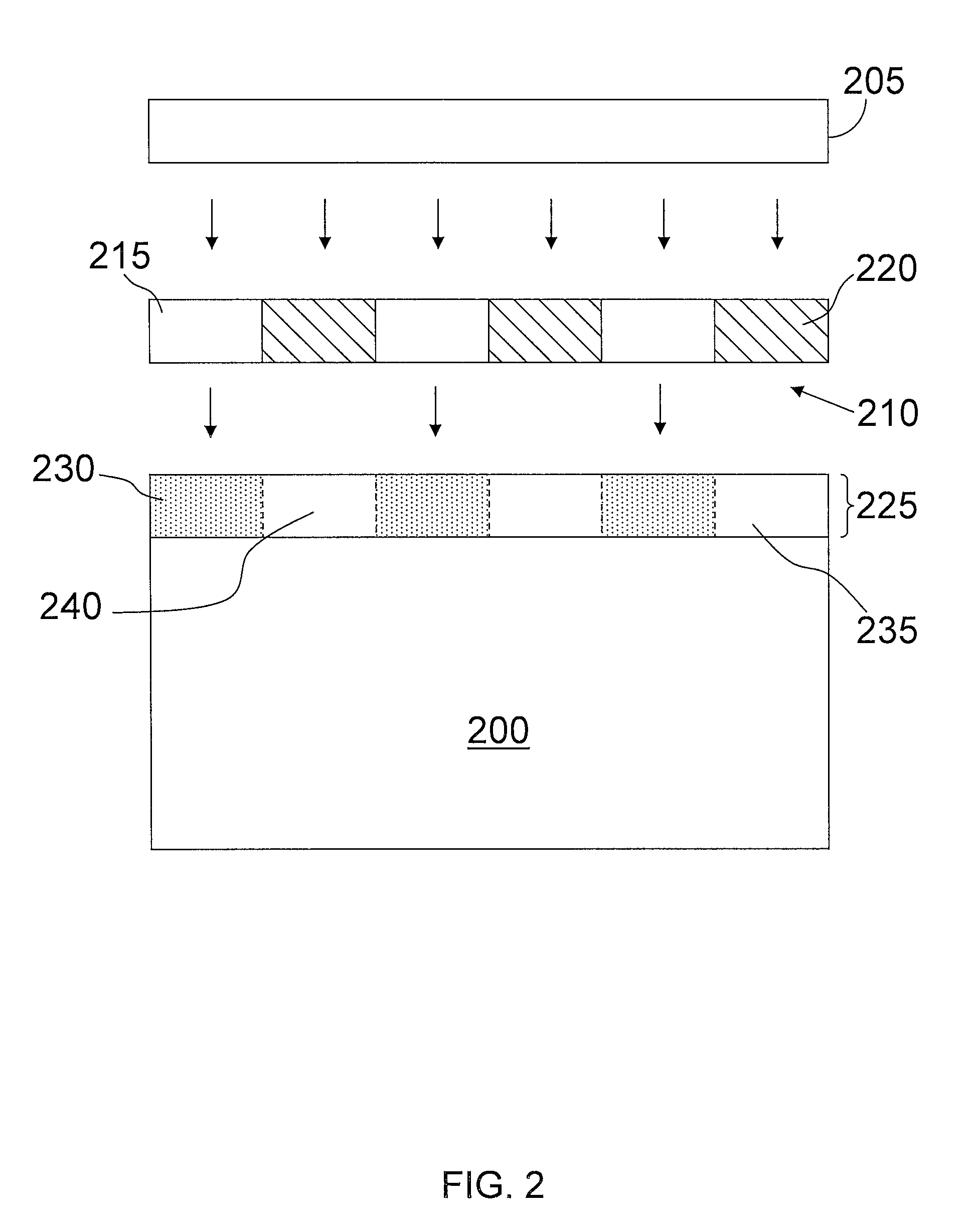
[0061]The patternable low-k composition was spin coated (30 seconds at 2000 rpm) onto an 8 inch silicon wafer to produce an approximately 0.6 μm film. The wafer and film were pre-exposure baked at about 110° C. for about 60 seconds (s), pattern-wise exposed to 248 nm deep ultraviolet (DUV) light on an ASML (0.63 NA, 5 / 8 annular) DUV stepper, and then post exposure baked at 110° C. for 60 s. This was followed by two 30 s puddle development steps with 0.26 N TMAH developer to resolve 0.250 μm li...


PUM

PropertyMeasurementUnit
Temperatureaaaaaaaaaa

Abstract

A method. The method includes dip coating a film of a composition on a silicon wafer substrate. The composition includes a polymer blend of a first polymer and a second polymer. The first polymer is a substituted silsesquioxane copolymer. The second polymer is a polysilsesquioxane having silanol end groups. The composition includes a photosensitive acid generator, an organic base, and an organic crosslinking agent. The film is patternwise imaged and at least one region is exposed to radiation having a wavelength of about 248 nanometers. The film is baked, resulting in inducing crosslinking in the film. The film is developed resulting in removal of base-soluble unexposed regions of the film, wherein a relief pattern from the film remains. The relief pattern is cured at a temperature between about 300° C. and about 450° C., and the curing utilizes a combination of thermal treatment with UV radiation.

Description

FIELD OF THE INVENTION[0001]The invention relates generally to on-chip electrical insulators used in integrated circuits, and more specifically, silicon-containing polymer blends as photopatternable dielectric materials.BACKGROUND OF THE INVENTION[0002]The continuous shrinking in dimensions of electronic devices utilized in ultra-large scale semiconductor integrated (ULSI) circuits in recent years may have resulted in increasing the resistance of the back-end-of-the-line (BEOL) metallization without concomitantly decreasing the interconnect capacitances. Interconnects may be scaled to higher aspect ratios (a height to width ratio of typically greater than 3:1) to mitigate the resistance increases, which may lead to increased capacitances. This combined effect may increase signal delays in ULSI electronic devices.[0003]The materials may be patterned by several patterning and sacrificial masking materials which may include photoresist polymers, via fill materials. Following the lithog...

Claims


Application Information

Patent Timeline
IPC IPC(8): B05D1/32C04B41/50
CPCG03F7/0382G03F7/0757G03F7/40H01L21/02137H01L21/02282H01L21/02348H01L21/3122H01L21/76802H01L21/76814H01L21/76825H01L21/76826H01L21/76828Y10S430/106Y10S430/108Y10S430/12Y10S430/121Y10S430/122Y10S430/126
Inventor ALLEN, ROBERT D.BROCK, PHILLIPDAVIS, BLAKE W.LIN, QINGHUANGMILLER, ROBERT D.NELSON, ALSHAKIMSOORIYAKUMARAN, RATNAM
Owner GLOBALFOUNDRIES INC
Why Eureka
Try Eureka