Graded PB for C4 bump technology

a bump technology and c4 technology, applied in the field of flip chip, can solve the problems of single nonrecurring read error on a single bit of a memory array, errors in devices on the semiconductor chip, and errors in radiation-sensitive devices

Inactive Publication Date: 2000-11-07
GLOBALFOUNDRIES INC
View PDF11 Cites 19 Cited by
  • Summary
  • Abstract
  • Description
  • Claims
  • Application Information

AI Technical Summary

Problems solved by technology

Although the use of such lead-based alloys allows for desirable processing conditions and reliable interconnect structures, the composition of the solder indirectly causes errors in devices on the semiconductor chip which are sensitive to radiation.
The emission of such alpha particles from the lead solder bump leads to errors in radiation-sensitive devices present on a semiconductor chip bonded to the solder bump.
Hence, an alpha particle may cause a single nonrecurring read error on a single bit of a memory array.
In other words, an alpha particle emitted from a solder bump is a potential source of soft errors.
Although perhaps the most direct solution to the problem, completely eliminating radioactive isotopes in solder bumps has proven to be both difficult and very expensive.
For instance, it is extremely difficult and costly to separate Pb.sup.210 from bulk lead.
Lead isotope separation necessitates the use of large, expensive instrumentation such as an accelerator.
Furthermore, because of its limited supply, it is very costly to use lead which naturally has a low abundance of the Pb.sup.210 isotope.
In fact, such "low-alpha" lead typically costs between fifty and sixty times the cost of lead normally used to form solder bumps.
In particular, error correction code is costly in that it creates memory redundancies and requires extra logic to implement.

Method used


Image

  • Graded PB for C4 bump technology
  • Graded PB for C4 bump technology
  • Graded PB for C4 bump technology

Examples


Embodiment Construction

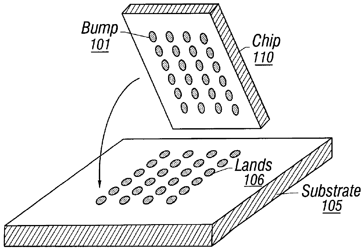
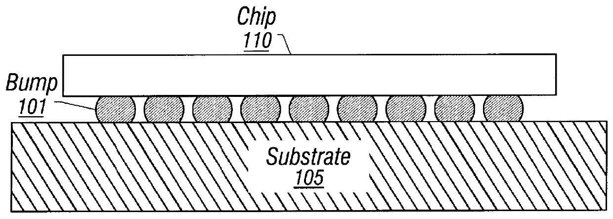
FIGS. 1A and 1B depict a flip chip interconnection of chip 110 to substrate 105 using solder bumps 101. Solder bumps 101 are formed on chip 110, then positioned and reflowed to form mechanical and electrical connections with matching wettable substrate lands 106 on substrate 105. In this way electrical connections can be provided for circuits on chip 110 to the outside world. Flip chip technology was developed during the 1960's by IBM and the current state of the art for flip chip and related chip scale semiconductor packaging technologies is described in a joint industry standard document, J-STD-012 entitled "Implementation of Flip Chip and Chip Scale Technology" and dated Jan. 19, 1996. Those of skill in the art will appreciate the techniques, materials, compositions, and methods of fabrication for such interconnect technology as described in the joint industry standard. J-STD-012 (January 1996) is incorporated herein by reference in its entirety.

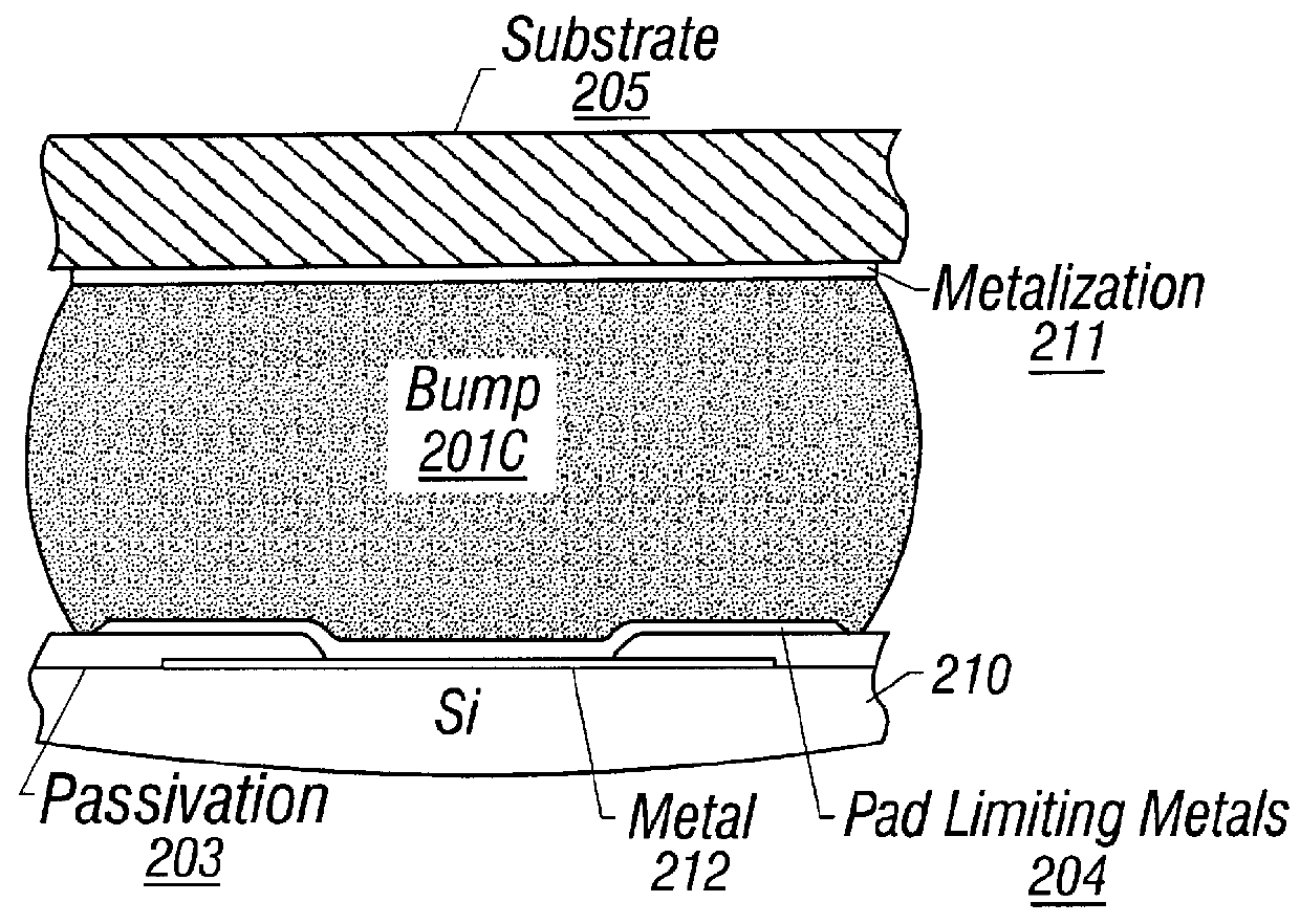
FIGS. 2A, 2B, and 2C depict solder...


PUM


Abstract

An improved solder bump composition and method advantageously employs a thin low-alpha layer of lead (Pb) deposited in close proximity to alpha particle sensitive devices, while ordinary (i.e., low cost) Pb is used for the bulk of the solder bump. This approach allows for reduced overall cost while still providing protection from alpha-particle induced soft errors. The low-alpha layer reduces the flux of alpha particle into devices in two ways. First, the low-alpha layer is itself essentially Pb210 free and therefore alpha particle emissions from the low-alpha layer are negligible. Second, the low-alpha layer is substantially opaque to alpha particles emitted by the ordinary Pb which includes Pb210. As a result, sensitive circuits on a semiconductor chip employing the improved solder bump are shielded from alpha particle emissions of the low-cost Pb210-containing portion of a solder bump.

Description

1. Field of the InventionThe present invention relates to semiconductor packaging technology, and more particularly to flip chip and related chip scale semiconductor packaging technology.2. Description of the Related ArtAs electronic devices become smaller and more dense, greater demands are placed on the ability to establish efficient, reliable interconnections from a semiconductor chip to a substrate. There are at least three known methods for interconnecting chips to substrates. Those three methods are face-up wire bonding, face-up tape-automated bonding, and the flip chip method. Of these three methods, the flip chip method has often been chosen as a preferred method for semiconductor packaging, for it allows for the interconnection of high-density devices having a large number of input and output paths. Specifically, the flip chip method is preferred because it provides short conductive leads from the chip to the substrate, a small device footprint, low inductance, high frequen...

Claims


Application Information

Patent Timeline
Patent Type & Authority Patents(United States)
IPC IPC(8): H01L23/48H01L23/552H01L23/485H01L23/556H05K3/34B23K35/26H01L21/60
CPCH01L23/556H01L24/10H01L24/13H01L2224/13099H01L2924/01012H01L2924/0102H01L2924/01029H01L2924/01049H01L2924/01051H01L2924/01056H01L2924/01061H01L2924/01074H01L2924/01079H01L2924/01082H01L2924/01092H01L2924/01105H01L2924/14H01L2924/19041H01L2924/30107H01L2924/3025H05K3/3463H01L2924/01006H01L2924/01024H01L2924/01033H01L2924/01084H01L2924/014H01L2924/00H01L24/03H01L24/05H01L2224/05001H01L2224/05022H01L2224/05572H01L2224/11502H01L2224/11849H01L2224/13H01L2924/00014H01L2224/05644H01L2224/05647H01L2224/05671H01L2224/05099H01L21/60
Inventor MILLER, ROY MARKMAILE, BERNDTIFFIN, DON A.HOSSAIN, TIM Z.
Owner GLOBALFOUNDRIES INC
Why Eureka
Try Eureka