Interlayer insulation of TFT LCD device having of silicon oxide and silicon nitride

a technology of silicon oxide and silicon nitride, which is applied in the field of interlayer insulation of tft lcd devices, can solve the problems of increasing the power consumption of the whole apparatus, affecting the image quality, and affecting the response time of the above-described tn liquid crystal display

Inactive Publication Date: 2000-12-12
SEMICON ENERGY LAB CO LTD
View PDF27 Cites 162 Cited by
  • Summary
  • Abstract
  • Description
  • Claims
  • Application Information

AI Technical Summary

Problems solved by technology

However, this increases the power consumption of the whole apparatus.
However, the response time of the above-described TN liquid crystal display is tens of milliseconds.
In this way, the image quality is not good.
In both TN and STN types, when the liquid crystal display is viewed obliquely, a decrease in contrast, inversion of intermediate color hues, and other undesirable phenomena are observed, because the state of polarization of light entering obliquely changes in the liquid crystal layer of the liquid crystal display.
In view of these problems, a method of dividing each pixel electrode into plural parts, a method of producing plural different states of orientation, and other methods have been proposed but no fundamental solution to the problems is available today.
This makes it impossible to realize a bright liquid crystal display.

Method used


Image

  • Interlayer insulation of TFT LCD device having of silicon oxide and silicon nitride
  • Interlayer insulation of TFT LCD device having of silicon oxide and silicon nitride
  • Interlayer insulation of TFT LCD device having of silicon oxide and silicon nitride

Examples


embodiment 2

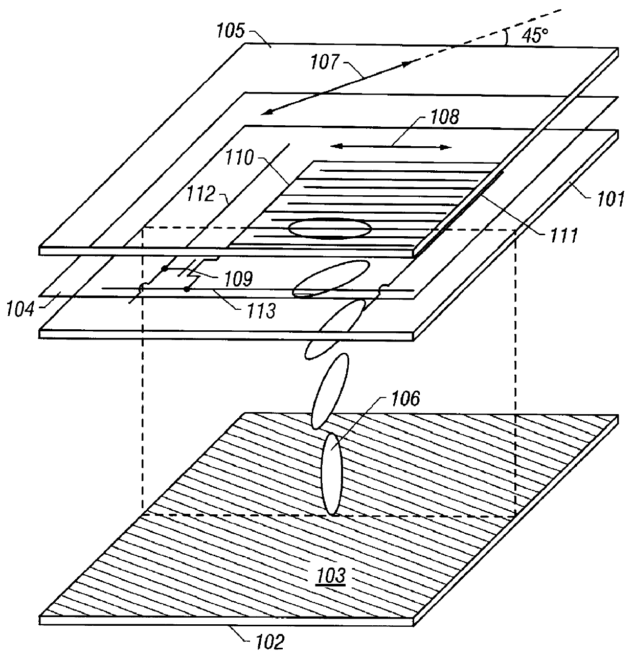
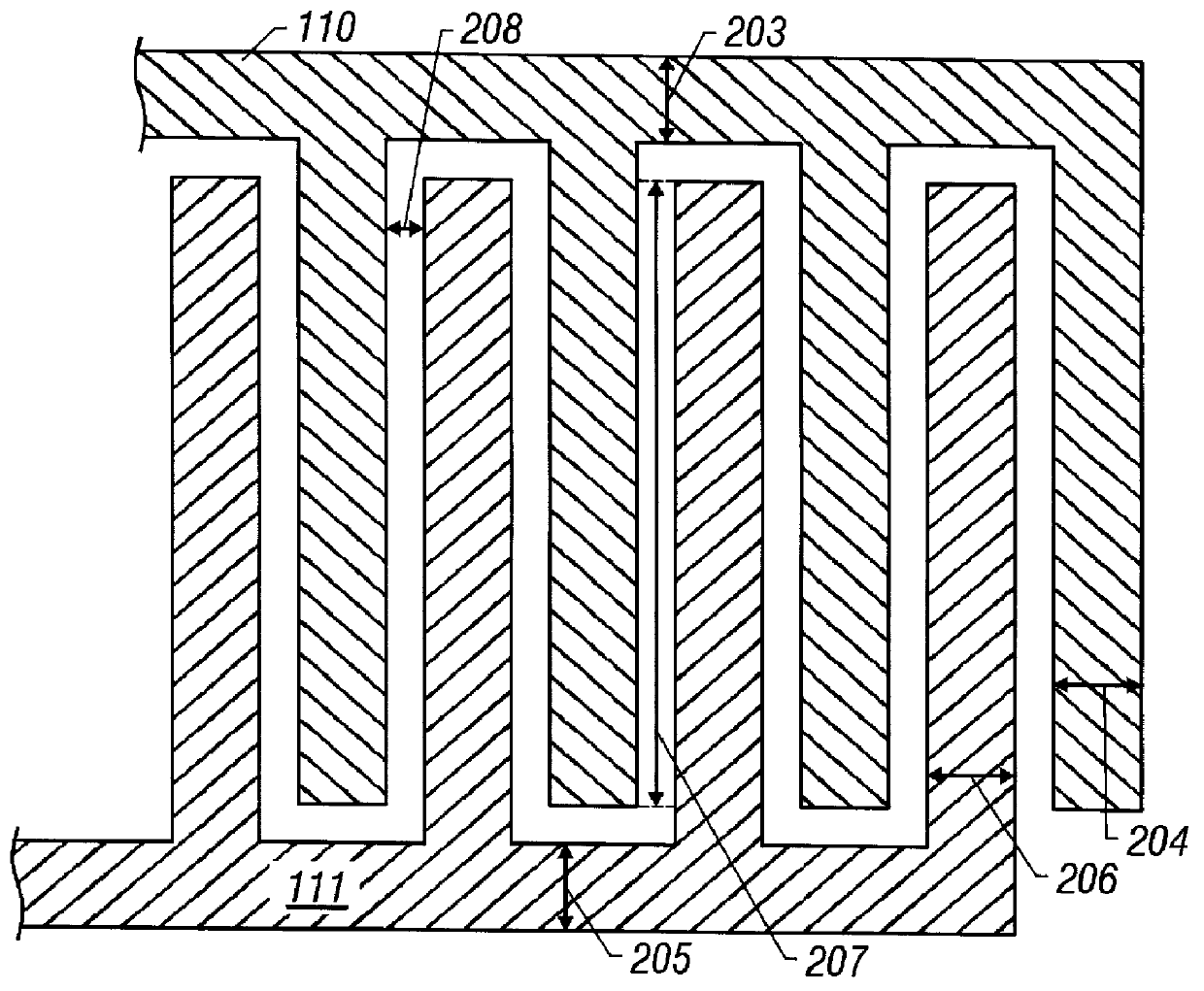
A method of fabricating a substrate for use in a liquid crystal display utilizing the active matrix circuit of the present embodiment is next described.

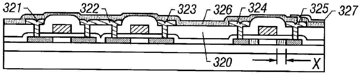
A process sequence for obtaining a monolithic active matrix circuit of the present embodiment is described below by referring to FIGS. 3(A)-3(F). This process sequence makes use of a low-temperature polysilicon process. The left sides of FIGS. 3(A)-3(F) show steps for manufacturing TFTs forming a driver circuit. The right sides show steps for manufacturing TFTs forming the active matrix circuit.

First, a glass substrate 301 was prepared as the first insulating substrate. A silicon oxide film was formed as a buffer oxide film 302 on the glass substrate 301 to a thickness of 1000 to 3000 .ANG. by sputtering techniques or plasma CVD in an oxygen ambient.

Then, an amorphous silicon film was formed to a thickness of 300 to 1500 .ANG., preferably 500 to 1000 .ANG., by plasma CVD or LPCVD. Thermal annealing was carried out above 500.degree. C...

embodiment 3

In the present embodiment, a color display was provided, using the liquid crystal display of Embodiment 2. As the pixel voltage applied across the liquid crystal display was varied, the intensity of transmitted light having a wavelength of 554.6 nm was varied. This is illustrated in FIG. 4. As can be seen from the graph of FIG. 4, the transmission varied continuously with varying the voltage. No clear threshold value existed. Variations in color hues were observed. When no voltage was applied, the device exhibited a color of yellow-green. When a voltage of 0.5 V was applied, it exhibited a color of green. When a voltage of 0.9 V was applied, it exhibited a color of blue. When a voltage of 1.2 V was applied, it exhibited a color of red.

A color display was provided, by making use of this phenomenon and by controlling the pixel voltage applied across the present embodiment of liquid crystal display. A multicolor display could be provided at an operating voltage of 3 V with a wide viewi...


PUM

PropertyMeasurementUnit
response timeaaaaaaaaaa
diameteraaaaaaaaaa
diameteraaaaaaaaaa

Abstract

There is disclosed a lightweight and small liquid crystal display which achieves low power consumption and in which the optical anisotropy of the liquid crystal material is compensated for in order to enhance the viewing angle characteristics and the response speed of the liquid crystal material. Display electrodes and a common electrode are formed on one of the substrates. The orientation of the liquid crystal material is of the HAN (hybrid alignment nematic) type. This compensates for the optical anisotropy of the liquid crystal material and improves the response speed.

Description

The present invention relates to an active matrix liquid crystal display.Since liquid crystal displays are lighter and more compact display devices than CRTs, they find extensive application in computers, electronic calculators, clocks, and watches. The principle of operation of liquid crystal displays depends on a change in an optical property, such as interference, scattering, diffraction, optical rotation, or absorption, of a liquid crystal material. This change is caused by a variation in orientation of the liquid crystal molecules or a phase transition in response to application of an external field such as electric field or heat.Generally, a liquid crystal display comprises a pair of substrates with a given spacing which is maintained at 1 to tens of micrometers. A liquid crystal material is held between these substrates, thus forming a liquid crystal panel. At least one of the substrates has transparency. Electrodes are formed on both or one of the substrates. Using these ele...

Claims


Application Information

Patent Timeline
Patent Type & Authority Patents(United States)
IPC IPC(8): G02F1/13G02F1/1362G02F1/1343G02F1/1337G02F1/136G09G3/36
CPCG02F1/134363G02F1/13306G02F1/13454G02F1/13363G02F1/1393G02F2203/02
Inventor YAMAZAKI, SHUNPEINISHI, TAKESHI
Owner SEMICON ENERGY LAB CO LTD
Why Eureka
Try Eureka