This helps you quickly interpret patents by identifying the three key elements:
Problems solved by technology
Method used
Benefits of technology
Benefits of technology
Tests have shown that this superficial film can make the stamping of incisions considerably easier, and allows much cleaner edges to be obtained at the rim of incisions with an equivalent depth of penetration, using an identical die.
By furthermore inserting an insulating material in the stamped incisions, for example a coating, adhesive, or the material of a laminated top layer, it is also possible to guarantee optimal insulation between adjacent turns.
Problems solved by technology
Such coils are complex to make, and therefore relatively costly.
Moreover the connection between the printed circuit and the coil gives rise to certain additional problems relating to mounting and poses problems of reliability, in particular when these elements are integrated in a chip card not offering adequate protection against deformation and mechanical stresses.
Furthermore the thickness of the coil makes it difficult to integrate the coil into a chip card of standard 0.76 mm thickness.
The tracks of the printed circuit are generally produced by photo-chemical means, which entails numerous costly operations and the use of polluting products.
This solution is complex to apply and entails, in particular, two distinct cutting operations.
It is difficult to obtain tracks of very narrow width with these stamping techniques.
Control of the temperature of the spike (3) poses additional difficulties; moreover, the metallic spike (3) must be moved slowly enough for the synthetic material to have time to melt.
This method is thus unsuitable for producing coils which must, for example, be integrated into chip cards and whose thickness as well as cost and production time must be minimized.
Method used
Image
Click on the blue label to locate the original text in one second.
Reading with bidirectional positioning of images and text.
Examples
first embodiment
FIG. 7, a perspective view of a chip card including a printed circuit according to the connection between the coil and an electronic component, both depicted in transparence;
second embodiment
FIG. 8, a perspective view of a chip card including a printed circuit according to the connection between the coil and an electronic component, both depicted in transparence.
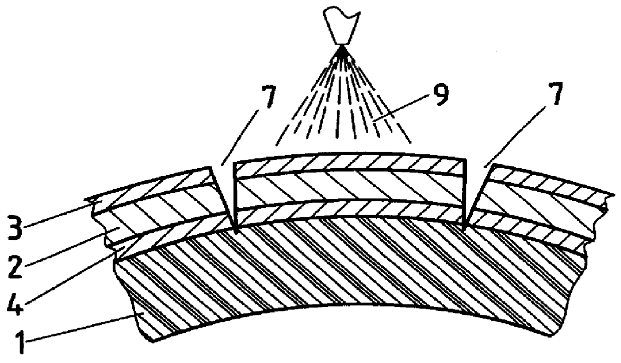
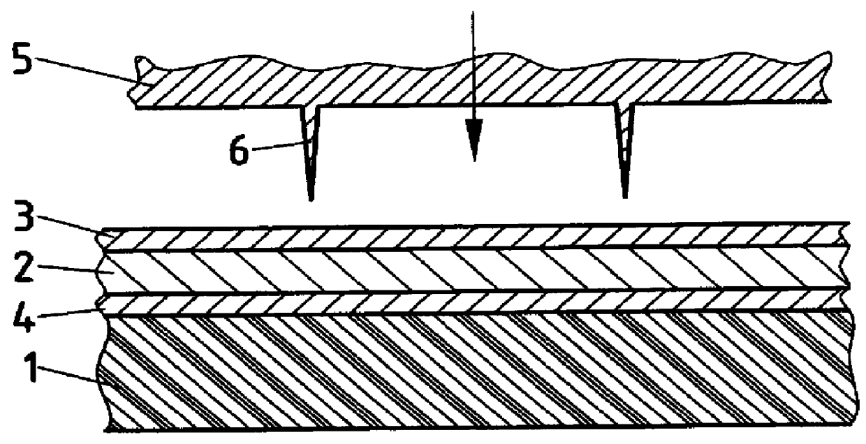
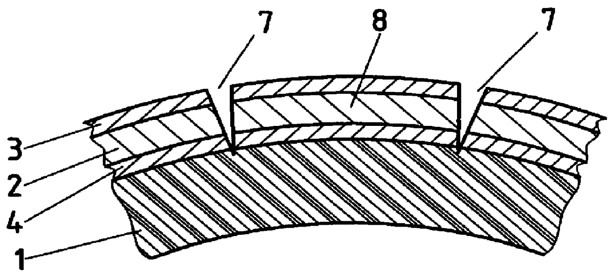
FIG. 1 shows a sectioned view of a sheet 1, 4, 2. The sheet 1, 4, 2 preferably consists of any dielectric substrate 1, for example a synthetic material of the PVC type or of cardboard, covered with a superficial conducting layer 2. Depending upon the application, a flexible film, or, on the contrary, a more rigid substrate will be chosen. The substrate 1 may thus consist of a composite or multi-layered material, for example a laminate comprising a number of layers of material, or include local reinforcements, for example of epoxy, fiberglass, carbon fiber, etc., for example in the region intended to receive the electronic component.
The superficial conducting layer 2 is applied to the layer 1 using a known method and is held in place, for example, by soldering or by means of adhesive 4. The adhesive 4 can, for ex...
third embodiment
In a third embodiment, this difference in height is compensated for beforehand by laminating over the dielectric 1, even before the application of the layer 2, 3, a dielectric sheet, not depicted, which was substantially the thickness of the layers 2, 3, 9, and whose shape corresponds to that of the portions without tracks A, B, C. In this case, the conducting layer 2, 3, is cut to the desired shape even before it is laminated on the layer 1.
The next manufacturing step, which is not illustrated here, involves mounting at least one electric or electronic component on the sheet 1, 2, 3, 4. This component can be fixed on the sheet by any means, for example by gluing or by bonding. In another embodiment, discussed in more detail further below, the component is simply placed at the appropriate place on the sheet and will be held in place only by the upper protective layer. Depending upon the thickness of the component, it could be necessary to provide a recess in the sheet 1, 2, 3, 4 to ...
PUM
Property
Measurement
Unit
Thickness
aaaaa
aaaaa
Electrical inductance
aaaaa
aaaaa
Electrical conductor
aaaaa
aaaaa
Abstract
PCT No. PCT / CH98 / 00231 Sec. 371 Date Oct. 25, 1999 Sec. 102(e) Date Oct. 25, 1999 PCT Filed Jun. 2, 1998 PCT Pub. No. WO98 / 56019 PCT Pub. Date Dec. 10, 1998A method of producing a transponder (20) comprising the following steps: demarcating the various turns (8) of a coil in a sheet (1), including a dielectric substrate covered by at least one conducting layer (2), by stamping said conducting layer with a stamping die (5) having sharp-edged surfaces (6) for contact with the superficial conducting layer (2; 2'''), connecting at least one electronic component (25) to the turns (8), and mounting at least one protective sheet (22; 27) covering the coil and the electronic component (25). To facilitate the stamping and to obtain clean incisions, the conducting layer is covered, before stamping, with a synthetic film. To prevent short circuits over the incisions, the incisions are preferably filled in with an adhesive, varnish or lacquer.
Description
The present invention relates to a method for producing transponder coils and to a transponder comprising a coil produced according to this method. More specifically, the present invention relates to a method of producing coils for transponders, for example for chip cards.PRIOR ARTIn the technology of transponders, and in particular of chip cards of the transponder type, it is often desired to connect an induction coil to an electronic circuit, such as, for example, an integrated circuit mounted on a printed circuit board. Such a configuration is described, for example, in WO-91 / 19302. The coil is generally produced by winding a wire around a core. Such coils are complex to make, and therefore relatively costly. Moreover the connection between the printed circuit and the coil gives rise to certain additional problems relating to mounting and poses problems of reliability, in particular when these elements are integrated in a chip card not offering adequate protection against deforma...
Claims
Application Information
Patent Timeline
Application Date:The date an application was filed.
Publication Date:The date a patent or application was officially published.
First Publication Date:The earliest publication date of a patent with the same application number.
Issue Date:Publication date of the patent grant document.
PCT Entry Date:The Entry date of PCT National Phase.
Estimated Expiry Date:The statutory expiry date of a patent right according to the Patent Law, and it is the longest term of protection that the patent right can achieve without the termination of the patent right due to other reasons(Term extension factor has been taken into account ).
Invalid Date:Actual expiry date is based on effective date or publication date of legal transaction data of invalid patent.

