Method of making high performance MOSFET with polished gate and source/drain feature

a high-performance, gate-polished technology, applied in the field of semiconductor processing, can solve the problems of low resistivity, adversely affecting the packing density and parasitic overlap capacitance between the gate, and polysilicon has the disadvantage of a much higher resistivity than aluminum

Inactive Publication Date: 2001-01-16
GLOBALFOUNDRIES INC
View PDF5 Cites 23 Cited by
  • Summary
  • Abstract
  • Description
  • Claims
  • Application Information

AI Technical Summary

Problems solved by technology

Aluminum was the material of choice due to its relatively low resistivity and material cost.
This alignment procedure can adversely affect both packing density and parasitic overlap capacitances between the gate and the source/drain regions.
Despite the several advantages of polysilicon over aluminum as a gate electrode material, polysilicon has the disadvantage of a much higher resistivity as compared to aluminum.
Higher resistivity translates into higher values of interconnect line resistance that can lead to undesirably long RC time constants and DC voltage variations within VLSI or ULSI circuits.
However, the resistivity of polysilicon gate electrodes in conventional MOS integrated circuit processing still presents a potential impediment to successful process scaling through reductions in the operating voltages of VLSI and ULSI devices.
Another disadvantage of polysilicon as a gate electrode material is polysilicon depletion.
If the amount of boron diffused is sufficiently high, the electrical performance of the field effect transistor may be severely degraded due to polysilicon depleti...

Method used


Image

  • Method of making high performance MOSFET with polished gate and source/drain feature
  • Method of making high performance MOSFET with polished gate and source/drain feature
  • Method of making high performance MOSFET with polished gate and source/drain feature

Examples


Embodiment Construction

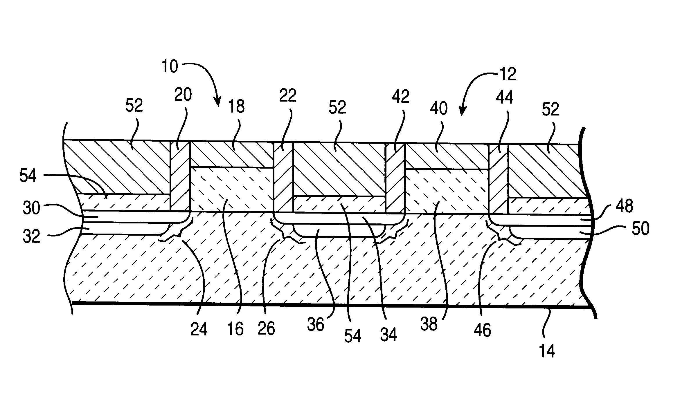
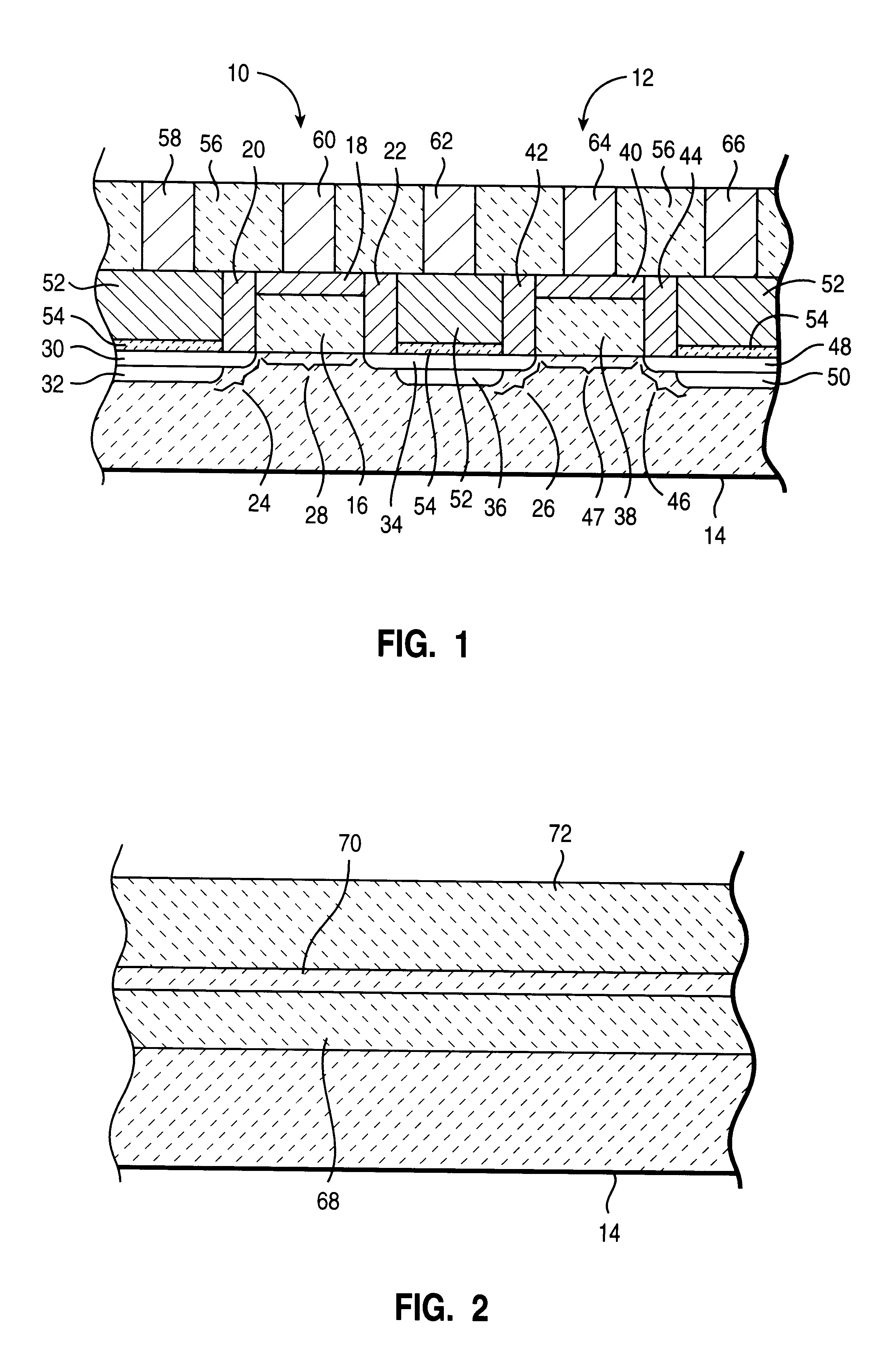
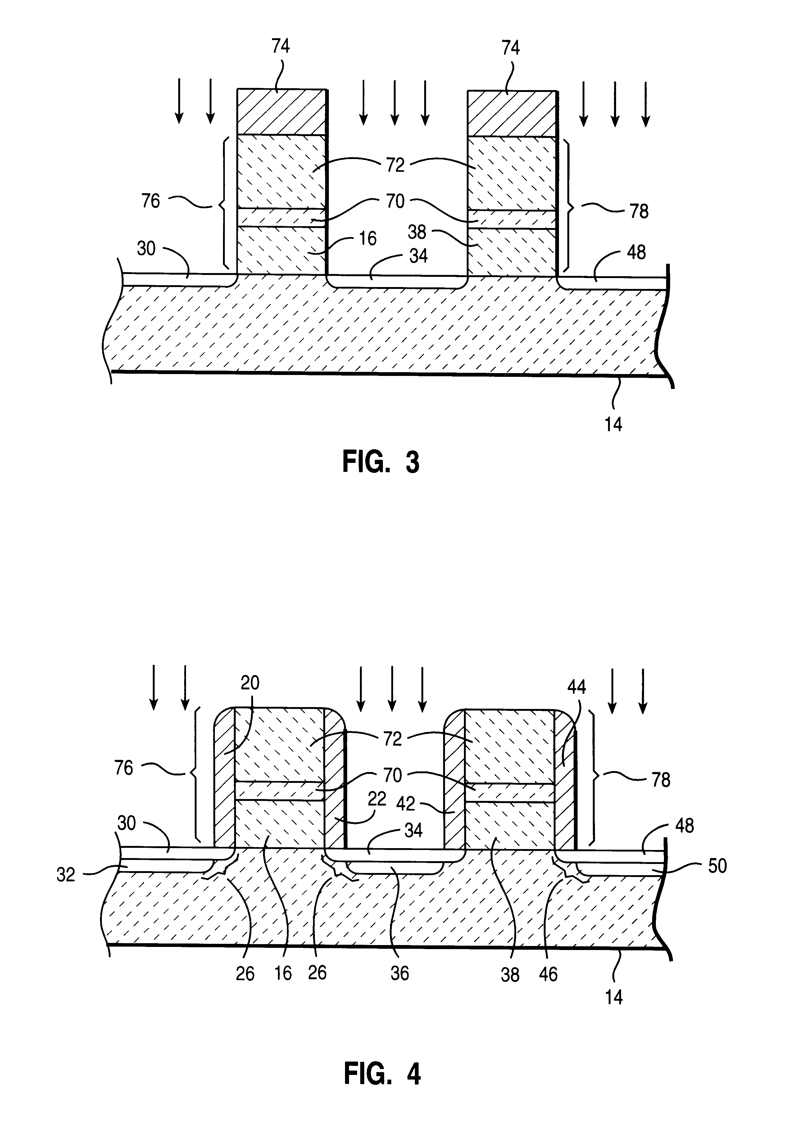
In the drawings described below, reference numerals are generally repeated where identical elements appear in more than one figure. Turning now to the drawings, and in particular to FIG. 1, there is shown a cross-sectional view of an exemplary embodiments of integrated circuit transistors 10 and 12 that are formed on a semiconductor substrate 14. The semiconductor substrate 14 may be composed of n-doped, or p-doped silicon, silicon-on-insulator, or other suitable substrate materials. The transistor 10 includes an insulating or gate dielectric layer 16 that is formed on the substrate 14 and a gate electrode 18 that is formed on the first insulating layer 16. A pair of insulating sidewall spacers 20 and 22 are positioned adjacent the gate dielectric layer 16. First and second source / drain regions 24 and 26 are formed in the substrate 14 and separated laterally to define a channel region 28 in the substrate 14 beneath the gate electrode 16. The source / drain region 24 consists of a ligh...


PUM


Abstract

A transistor and a method of making the same are provided. The method includes the steps of forming a gate dielectric stack on the substrate that has a gate dielectric layer and forming first and second sidewall spacers adjacent the gate dielectric stack. A first portion of the gate dielectric stack is removed while a second portion thereof is left in place. First and second source/drain regions are formed in the substrate, and a conductor layer is formed over the first and second source/drain regions and on the second portion of the gate dielectric stack. The gate dielectric may be composed of a high dielectric constant material with a thin equivalent thickness of oxide. The method enables integrated processing of the gate electrode and source/drain metallization.

Description

1. Field of the InventionThis invention relates generally to semiconductor processing, and more particularly, to an integrated circuit transistor with integrated gate electrode and source / drain metallization, and to a method of making the same.2. Description of the Related ArtA typical field effect transistor implemented in silicon consists of a source and a drain formed in a silicon substrate, and separated laterally to define a channel region in the substrate. A gate electrode composed of a conducting material, such as aluminum or polysilicon, is disposed over the channel region and designed to emit an electric field into the channel region. Changes in the electric field emitted by the gate electrode enable, or alternatively, disable the flow of current between the source and the drain.In a conventional process flow for forming a typical field effect transistor, a gate oxide layer is grown on a lightly doped silicon substrate and a layer of polysilicon is deposited on the gate oxi...

Claims


Application Information

Patent Timeline
IPC IPC(8): H01L21/70H01L21/28H01L21/285H01L21/02H01L21/768H01L29/51H01L21/336H01L29/40
CPCH01L21/28167H01L21/28518H01L21/7684H01L21/76877H01L29/51H01L29/66545H01L21/28194H01L29/6659
Inventor GARDNER, MARK I.GILMER, MARK C.
Owner GLOBALFOUNDRIES INC
Why Eureka
Try Eureka