Silicon single crystal wafer and method for producing it

a single crystal wafer and silicon technology, applied in the direction of semiconductor/solid-state device testing/measurement, instruments, under a protective fluid, etc., can solve the problems of low yield in the v-rich region, lowered device yield, and used device fabrication

Inactive Publication Date: 2001-02-20
SHIN-ETSU HANDOTAI CO LTD
View PDF11 Cites 37 Cited by
  • Summary
  • Abstract
  • Description
  • Claims
  • Application Information

AI Technical Summary

Problems solved by technology

Further, the N-region is on an I-rich region side, and is not rich enough to cause formation of LSEPDs and LFPDs (See FIG. 5, line (B), FIG. 6(B)).
Particularly, not in a test machine but in a machine for actual production, it is difficult to control precisely, and therefore, there is a problem in productivity, and such a method is not practical.
However, in a device process, yield is low in V-rich region although high in N-region.
However, it is not used for fabrication of device, sinc...

Method used


Image

  • Silicon single crystal wafer and method for producing it
  • Silicon single crystal wafer and method for producing it
  • Silicon single crystal wafer and method for producing it

Examples


example 1

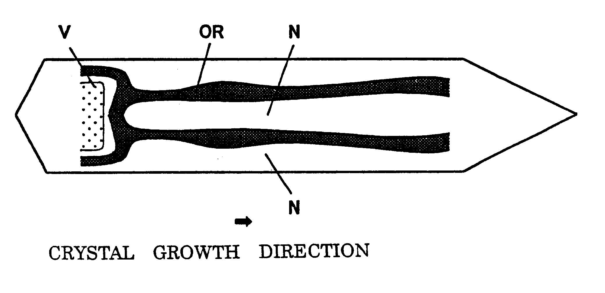
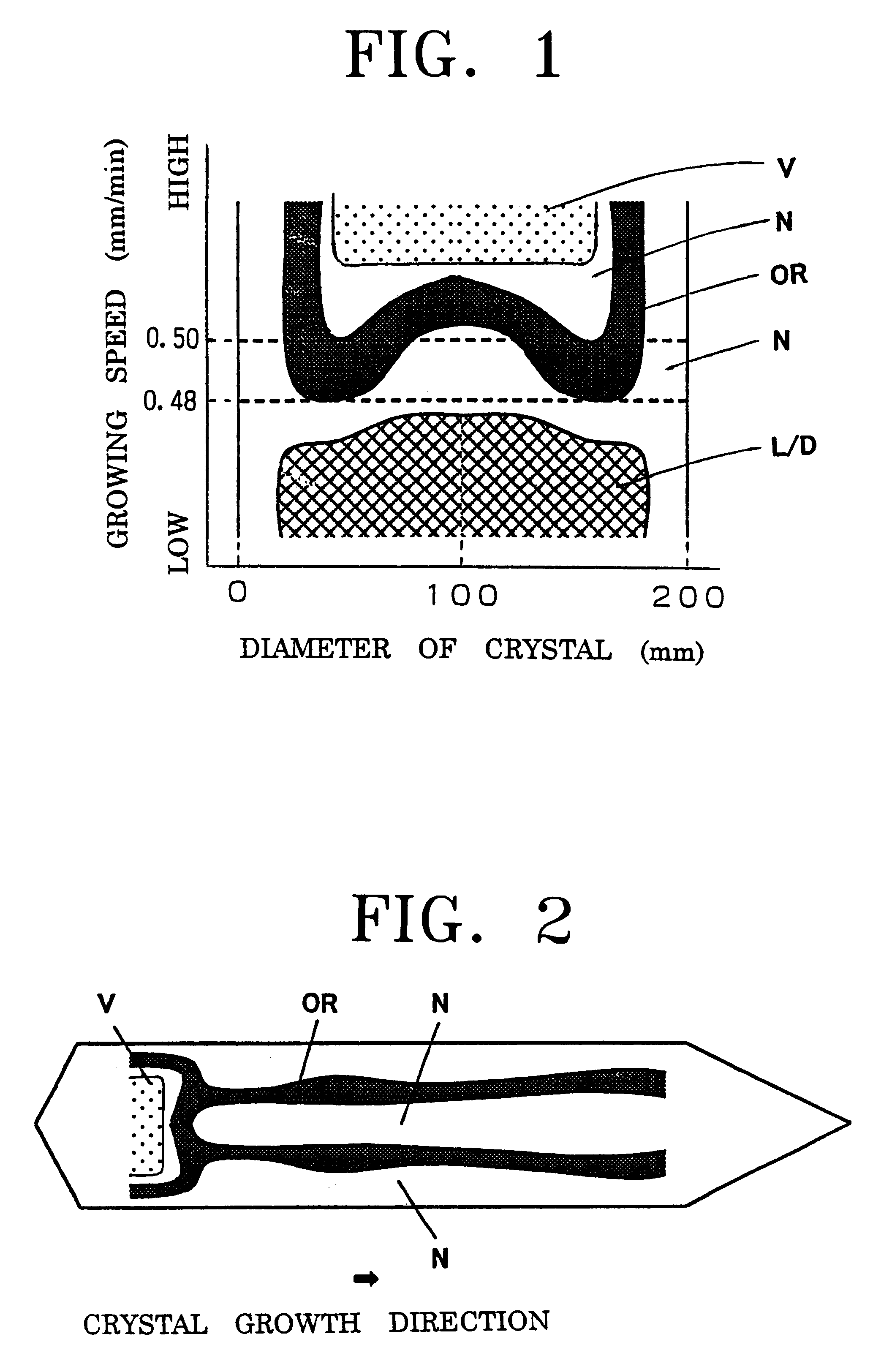
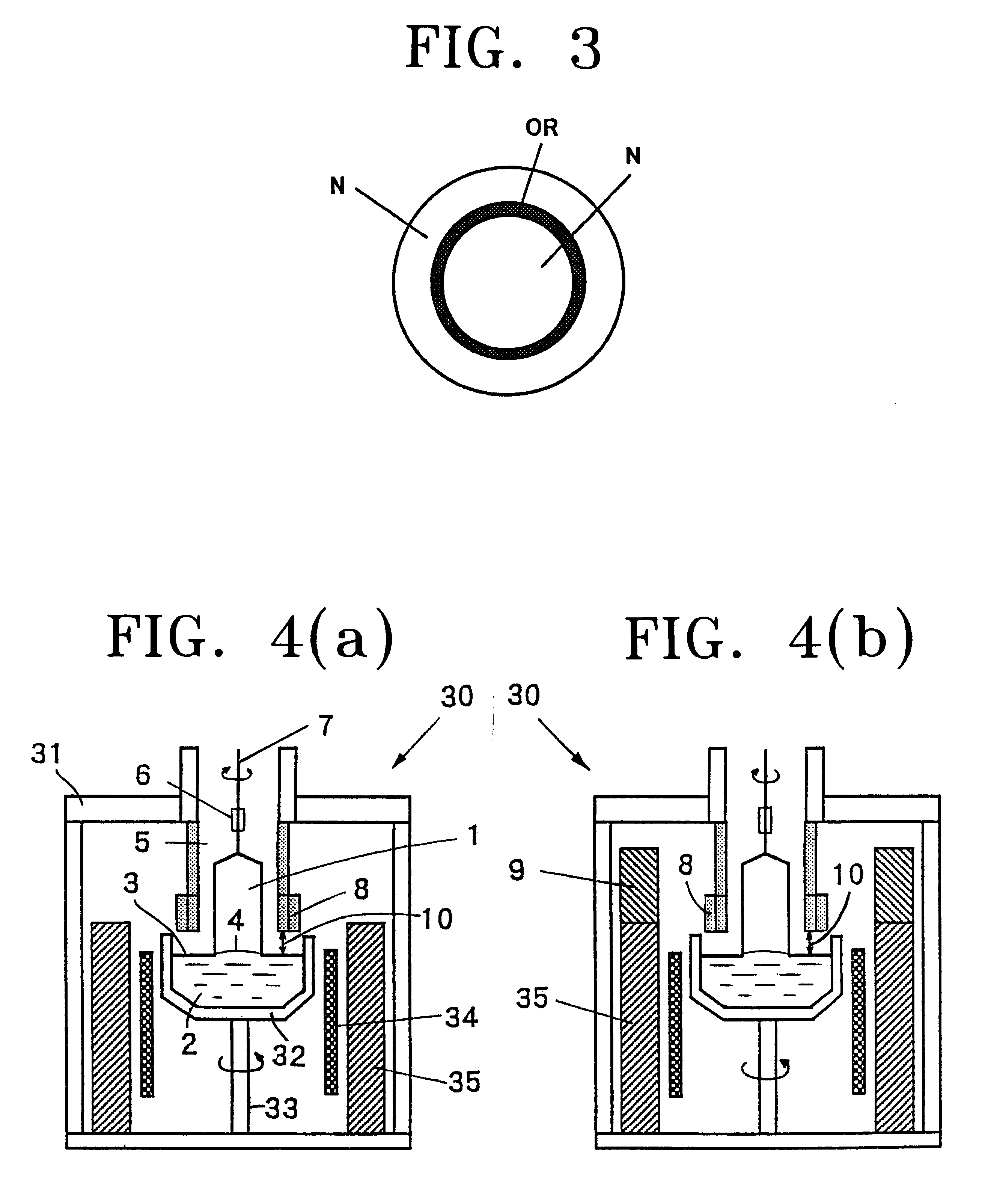
A silicon single crystal was grown through use of the crystal pulling apparatus 30 of FIG. 4(a). 100 kg of Polycrystalline material of silicon was charged into a quartz crucible having a diameter of 24 inches. A single crystal ingot having a diameter of 8 inches and a length in the straight body of about one meter and orientation was pulled.

The furnace structure (hot zone: HZ) wherein a gap 10 between the surface 3 of the silicon melt and the lower end of the annular solid-liquid interface insulator 8 was 70 mm was used. The temperature of the silicon melt 2 was kept at about 1420.degree. C.

The average pulling rate was decreased under the following condition, from 0.6 to 0.3 mm / min, by 0.05 mm / min every tenth centimeter, and elimination of OSF ring at the center of a bulk of crystal and formation of L / D region were studied. The crystal was cut vertically at a thickness of 2 mm, and subjected to an etching treatment in order to eliminate a surface mechanical damage to prepare two sa...

example 2

The crystal was pulled in the same manner as Example 1 except that the furnace structure wherein the upper insulator 9 was disposed on the insulating material 35 was provided as shown in FIG. 4(b), and a gap 10 between the surface 3 of the silicon melt and the lower end of the annular solid-liquid interface insulator 8 was 60 mm. The single crystal ingot having almost the same quality as Example 1 was obtained. In that case, the OSF region was apt to be narrower in the surface of the wafer, since .DELTA.G was shifted further to minus side.

example 3

The crystal was pulled in the same manner as Example 1 except that oxygen concentration in the growing crystal was controlled to be 24 ppma or less. The defects were evaluated. OSF was not generated when thermal oxidation was performed. It is considered that latent nuclei were present, but OSF was not generated when thermal oxidation was performed, since oxygen concentration was low.

The present invention is not limited to the above-described embodiment. The above-described embodiment is a mere example, and those having the substantially same structure as that described in the appended claims and providing the similar action and effects are included in the scope of the present invention.

For example, in the above-described embodiment, the silicon single crystal having a diameter of 8 inches was grown. However, the present invention can be applied to a method of pulling a crystal recently produced having larger diameter, for example, 10 to 16 inches, or more. Furthermore, the present i...


PUM


Abstract

There is disclosed a method for producing a silicon single crystal in accordance with the Czochralski method wherein a crystal is pulled with controlling a temperature in a furnace so that DELTAG may be 0 or a negative value, where DELTAG is a difference between the temperature gradient Gc (° C./mm) at the center of a crystal and the temperature gradient Ge (° C./mm) at the circumferential portion of the crystal, namely DELTAG=(Ge-Gc), wherein G is a temperature gradient in the vicinity of a solid-liquid interface of a crystal from the melting point of silicon to 1400° C., and with controlling a pulling rate in a range between a pulling rate corresponding to a minimum value of the inner line of OSF region and a pulling rate corresponding to a minimum value of the outer line, when OSF region is generated in an inverted M belt shape in a defect distribution chart which shows a defect distribution in which the horizontal axis represents a diameter of the crystal and the vertical axis represent a pulling rate. There can be provided a method of producing a silicon single crystal wafer by CZ method wherein OSF in the ring shape distribution generated when being subjected to thermal oxidation or latent nuclei of OSF is present in a low density, and neither FPD, COP, L/D, LSTD nor defect detected by Cu decoration is present under a stable manufacture condition.

Description

1. Field of the InventionThe present invention relates to a silicon single crystal wafer having few crystal defects, as well as to a method for producing it.2. Description of the Related ArtAlong with a decrease in size of semiconductor devices for achieving an increased degree of integration of semiconductor circuits, more severe quality requirements have recently been imposed on silicon single crystals which are grown by the Czochralski method (hereinafter referred to as the CZ method) for use as materials for substrates of semiconductor devices. Particularly, there has been required a reduction in density and size of grown-in defects such as FPDs, LSTDs, and COPs, which are generated during the growth of a single crystal and degrade oxide dielectric breakdown voltage and characteristics of devices.In connections with the above-mentioned defects incorporated into a silicon single crystal, first are described factors which determine the concentration of a point defect called a vaca...

Claims


Application Information

Patent Timeline
IPC IPC(8): C30B15/00C30B15/14C30B15/22C30B15/20C30B29/06G01N21/00G01N21/27G01N21/88G05D23/19H01L21/208H01L21/66
CPCC30B15/14C30B15/203C30B29/06Y10S117/917C30B15/00
Inventor SAKURADA, MASAHIROYAMANAKA, HIDEKIOHTA, TOMOHIKO
Owner SHIN-ETSU HANDOTAI CO LTD
Why Eureka
Try Eureka