

Semiconductor micromachine and manufacturing method thereof
a micromachine and semiconductor technology, applied in the direction of acceleration measurement using interia force, turn-sensitive devices, instruments, etc., can solve the problems of crosstalk of signals, low degree of design freedom of circuits, and observation of the same drawbacks as in the angular velocity sensor
- Summary
- Abstract
- Description
- Claims
- Application Information
AI Technical Summary
Problems solved by technology
Method used
Image

Examples
first embodiment
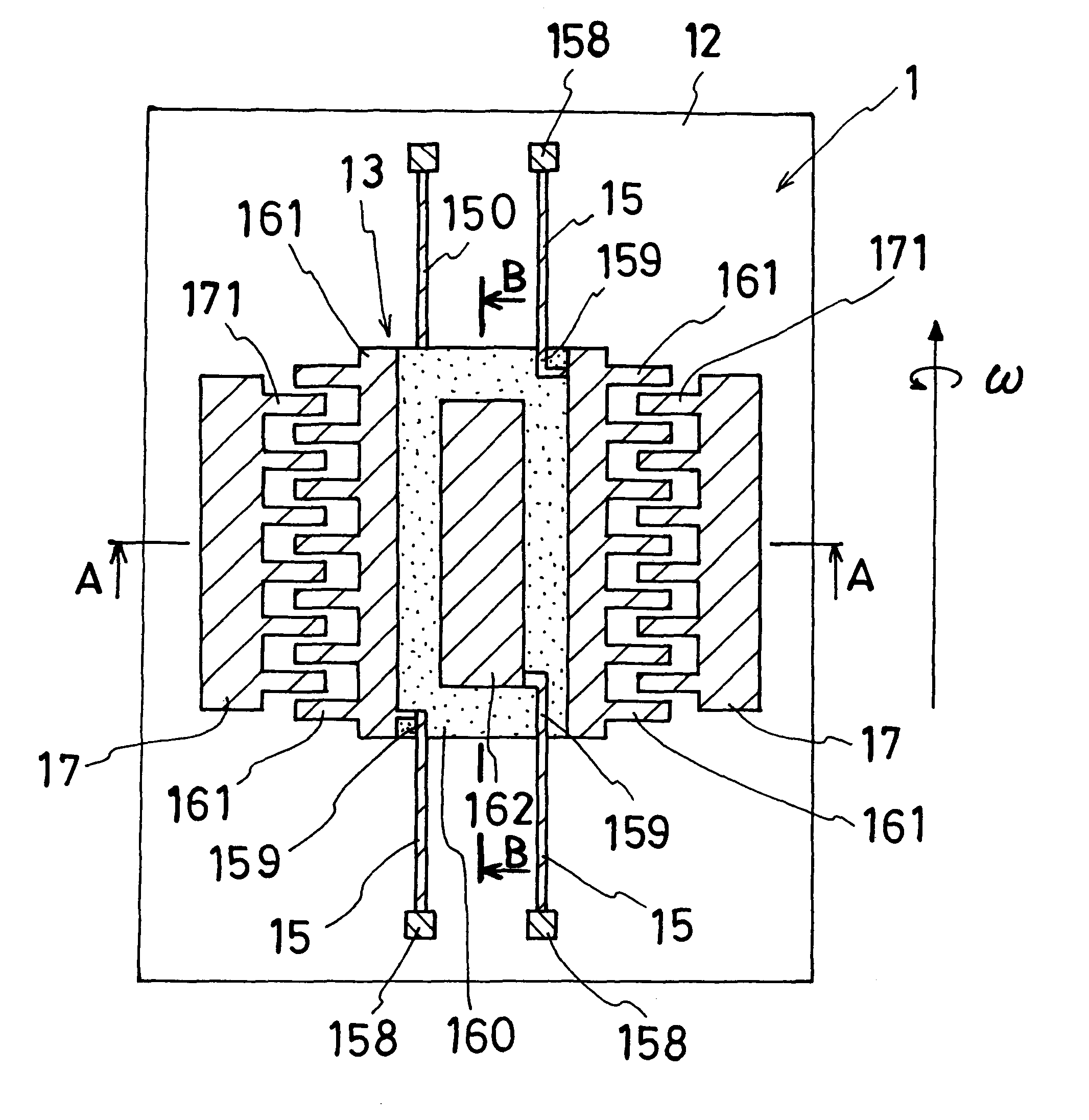
A semiconductor micromachine according to a first embodiment of the present invention will be described with reference to FIGS. 1, 2. The semiconductor micromachine of this embodiment is an angular velocity sensor manufactured by using micromachining technology, and the basic structure thereof is substantially the same as that of the conventional semiconductor micromachine (See FIGS. 15 through 17).
As shown in FIGS. 1, 2, the semiconductor micromachine 1 of this embodiment has a substrate 12 and a movable portion 13. The movable portion 13 is composed of a polycrystalline silicon thin film supported by acicular bodies 15, 150, and is arranged opposite the substrate 12 with a gap 11 provided therebetween. Provided in the movable portion 13 are an electrode and wires 159. The electrode is composed of movable-side driving electrode sections 161 and movable side detecting electrode section 162. The respective electrode sections and wires are interconnected by an electrical insulation se...
second embodiment
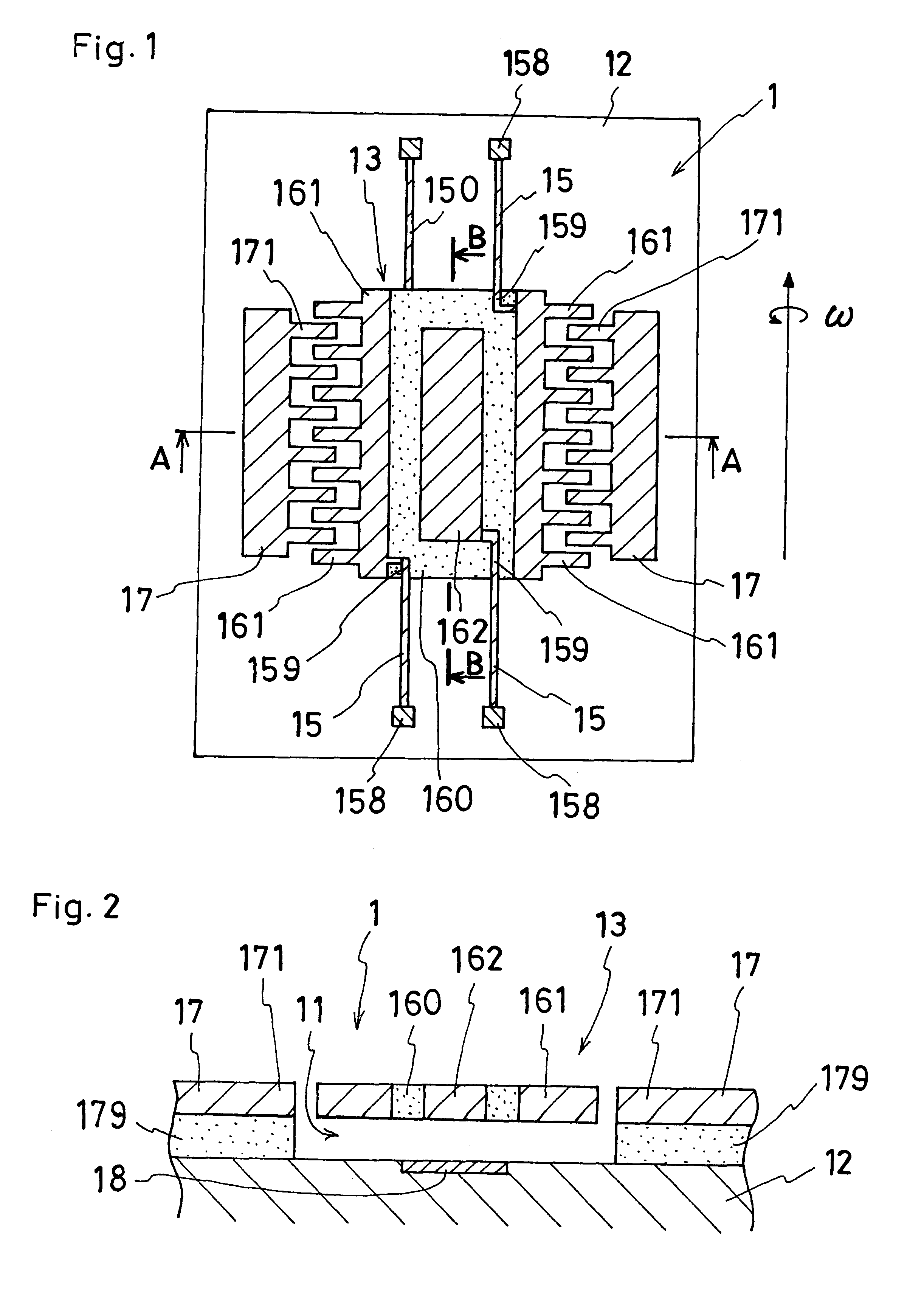
A semiconductor micromachine according to a second embodiment of the present invention will now be described.
The semiconductor micromachine 19 as illustrated in FIG. 3 includes the movable portion 13, which has on both sides thereof the comb-shaped driving electrode sections 161. The detecting electrode section 162 constitutes a central portion of the movable portion 13. The movable portion 13 is also provided with the wires 159 for electrically connecting the detecting and driving electrode sections 162, 161 with the acicular bodies 15.
The driving electrode sections 161, the detecting electrode section 162, and the wires 159 are interconnected by the electrical insulation section 160.
The movable portion 13 is made of an undoped polycrystalline silicon, while the driving electrode sections 161, the detecting electrode section 162, and the wires 159 are each made of an n-type semiconductor manufactured by doping the aforementioned polycrystalline silicon using ion implantation of pho...
third embodiment
A semiconductor micromachine according to third embodiment of the present invention will now be described.
The semiconductor micromachine of this embodiment is basically identical to that of the first embodiment except that a diffusion inhibiting layer 50 is formed on a bottom surface of the movable portion 13 facing the gap portion 11 as illustrated in FIG. 6(b). A concrete construction of this embodiment is apparent from FIGS. 1, 2 for illustration of the first embodiment, and hence, the explanation thereof is omitted.
The overall manufacturing method of this semiconductor micromachine will now-be described with reference to FIGS. 5 through 8.
First, the substrate 12 having on a surface thereof an oxidation film 53 and an etching stopper layer 54 is prepared. Subsequently, an etching layer 55 is then provided on the etching stopper layer 54. A diffusion inhibiting layer 50 is then provided on the etching layer 55, and a semiconductor thin film 57 is then provided on the diffusion inh...
PUM
| Property | Measurement | Unit |
|---|---|---|
| side length | aaaaa | aaaaa |
| thickness | aaaaa | aaaaa |
| thickness | aaaaa | aaaaa |
Abstract
Description
Claims
Application Information