
Driver circuit and method of operating the same

Inactive Publication Date: 2001-03-06
TELEFON AB LM ERICSSON (PUBL)
View PDF10 Cites 48 Cited by
  • Summary
  • Abstract
  • Description
  • Claims
  • Application Information

AI Technical Summary

Benefits of technology

It is a further object of the present invention to provide a driver circuit for driving at least two functional means which, when the components thereof are mounted on a PCB, requires little time by a resource for mounting the components on the PCB, such as a pick-and-place machine.
It is a further object of the present invention to provide a driver circuit for driving a number of functional means which are controlled through a small number of control signal lines. It is an object of the present invention to have a smaller number of control signal lines than the number of functional means thereby allowing a small number of output ports of a control unit to be used with the result that the output ports and the control signal lines require, when implemented, a small space on a PCB.
This construction achieves the advantage that the space on a PCB required by two or more drivers is smaller than when the same number of drivers are realized separately since a smaller number of components are required.
Furthermore, the construction achieves the advantage that, when the components of the driver circuit for driving at least two functional means are mounted on a PCB, less time is required by a resource for mounting the components on a PCB, such as a pick-and-place machine, since a smaller number of components are required compared to when the same number of drivers are realized separately.
Furthermore, the construction achieves the advantage that a smaller number of signals for controlling the drivers are required compared to the number of signals for controlling the same number of drivers when these are realized separately.
The smaller space required on the PCB is the result of the fact that a smaller number of components (inductors and switches) are needed for the driver circuit of the present invention compared to the number of components needed for the prior art drivers when the same amount of drivers are used. Furthermore, the required space on the PCB is also reduced due to the fact that a smaller number of control signal lines need to be realized on the PCB. When these control signal lines are generated by output ports of for example a micro-processor the PCB space required is further reduced because a smaller number of output ports need to be realized on the PCB. The smaller number of control signal lines and possibly the number of output ports required is also a result of the method of operating the driver circuit of the present invention where the operation of more than one functional means may be controlled by the use of one control signal by changing the frequency of the control signal.

Problems solved by technology

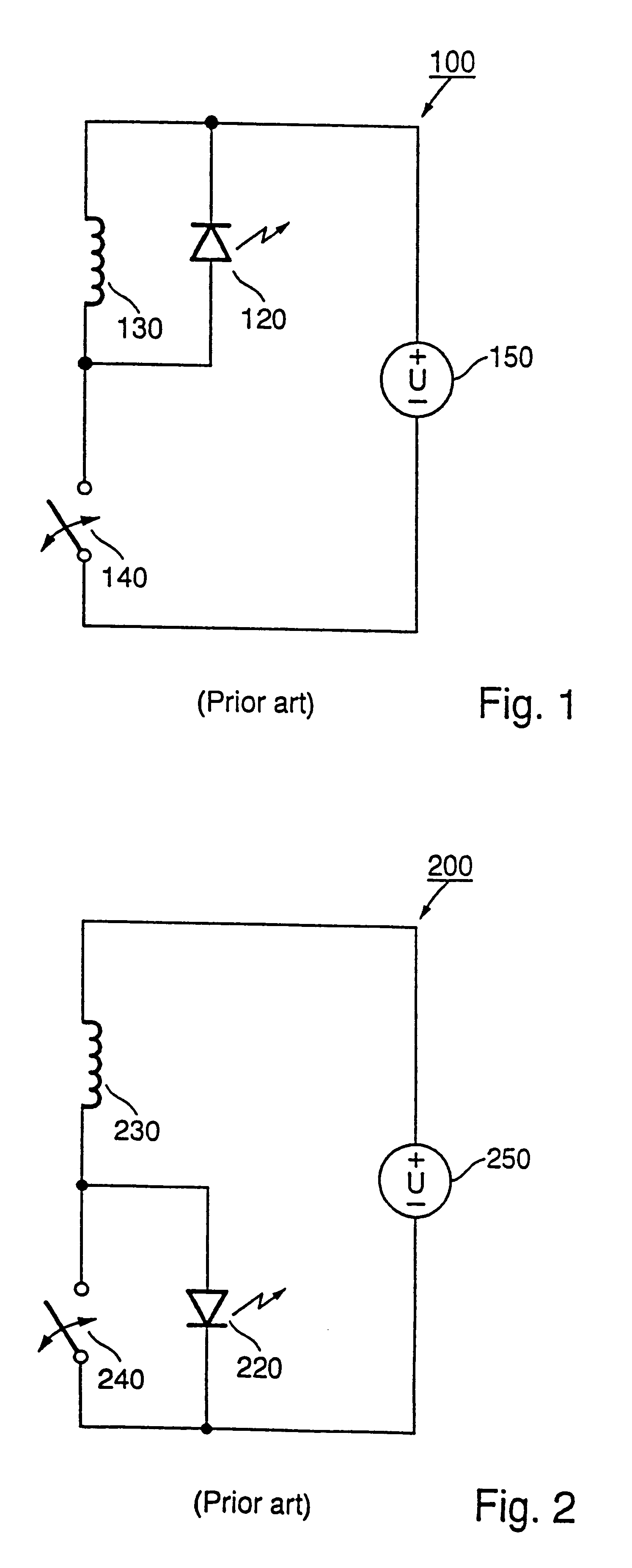
A drawback with the first type of LED driver is that the LED requires a minimum voltage in the forward direction to emit light.
Furthermore, the current limiting resistor will consume power which will be wasted.
These drawbacks become more pronounced when the voltage source is a battery where the maximum voltage supplied is limited and the energy stored in the battery is a scarce resource.
In this case it would not be possible to use a battery providing a voltage of 1.5 V. The situation becomes even worse if two or more LED's are connected in series.
Even if the voltage of the voltage source is sufficiently high to allow the LED to emit light, energy is wasted in the resistor.
This is undesired since the available amount of energy which is stored in the battery is limited.
Furthermore, this solution does not include any current limiting resistor in which power is wasted.
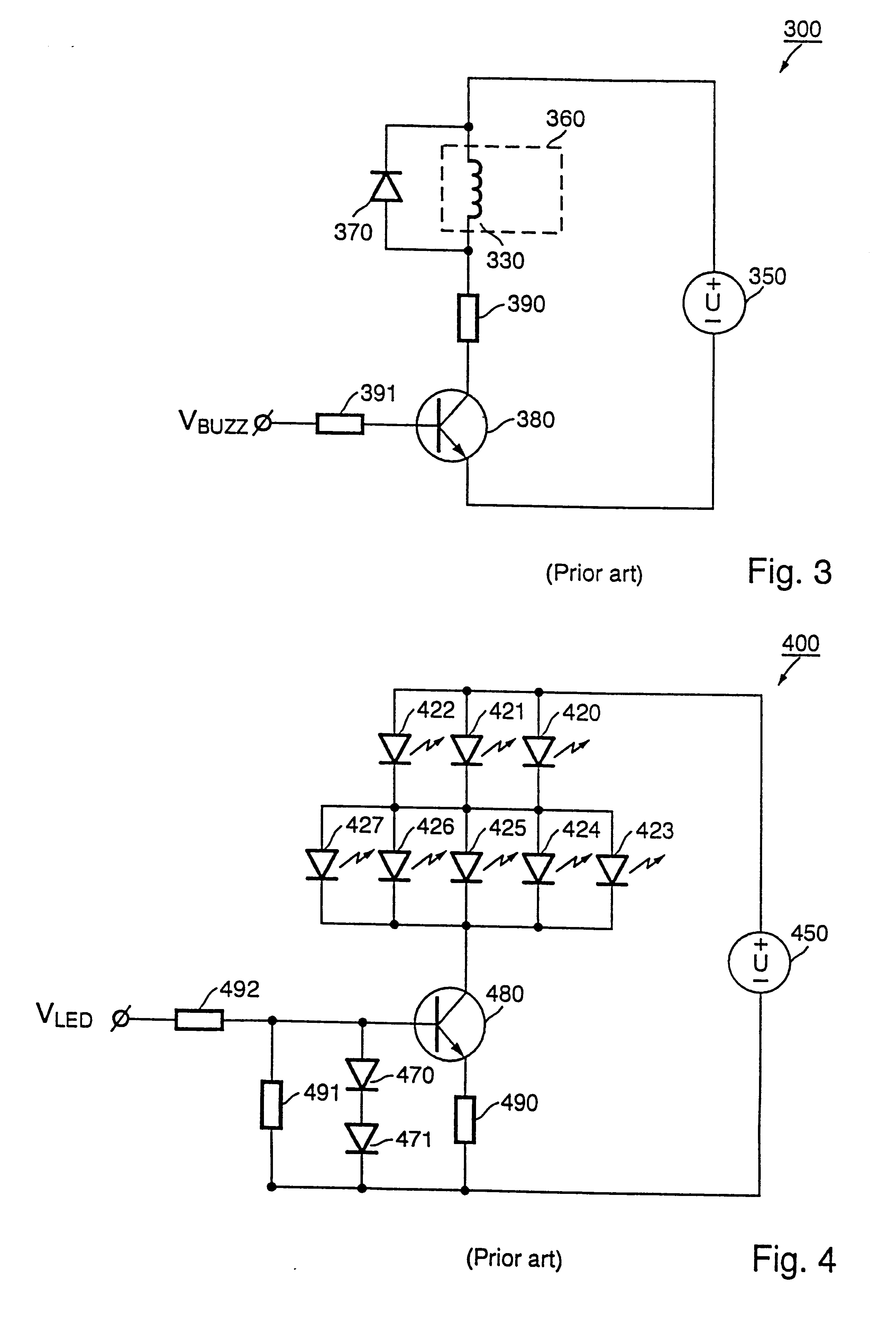
A problem with the prior art drivers is that if more than one of the drivers are realized in a common system the total space required by the driver circuits on a Printed Circuit Board, PCB, is large.
This problem becomes more acute when several driver circuits are realized in a system which need to have physically small dimensions.
A further problem with the prior art drivers when they are realized in a common system is that the mounting of the components on a PCB, for example by a pick-and-place machine, takes at least the time it takes to mount all the components of each driver sequentially.
The time it takes to mount a component on a PCB corresponds to a cost since a resource, such as a pick-and-place machine, will be occupied during the period of time it takes to mount the component.
A further problem with the prior art drivers when they are realized in a common system is that each of the drivers requires a separate control signal for controlling the operation of the driver.
In many systems the number of output ports of the control unit is a scarce resource.
This problem becomes even more acute when the control unit is to be fitted into a physically small application, such as a handheld system, because each output port occupies a certain minimum area on the PCB.

Method used


Image

  • Driver circuit and method of operating the same
  • Driver circuit and method of operating the same
  • Driver circuit and method of operating the same

Examples


first embodiment

FIG. 8 illustrates a circuit diagram of an LED and buzzer driver 1000 according to the present invention. The driver comprises a voltage source 1050 connected to first and second connection points (not shown), a buzzer 1060, a switch 1040 and four LED's 1020-1023. The buzzer 1060 comprises an inductor 1030 as described above. A first electrode of the inductor 1030 is connected to the electrode of the voltage source 1050 having the most positive potential, "plus-pole". A second electrode of the inductor 1030 is connected to a first electrode of the switch 1040 and to the anodes of the first and third LED's 1020, 1022. The cathodes of the first and third LED's 1020, 1022 are connected to the anodes of the second and fourth LED's 1021, 1023, respectively. The cathodes of the second and fourth LED's 1021, 1023 and a second electrode of the switch 1040 are connected to the electrode of the voltage source 1050 having the most negative potential, "minus-pole".

In operation, the switch 1040 ...

second embodiment

FIG. 9 illustrates a circuit diagram of an LED and buzzer driver 1100 according to the present invention. The driver comprises a voltage source 1150 connected to first and second connection points (not shown), a buzzer 1160, a switch 1140 and four LED's 1120-1123. The buzzer 1160 comprises an inductor 1130 as described above. A first electrode of the switch 1140 is connected to the electrode of the voltage source 1150 having the most positive potential, "plus-pole". A second electrode of the switch 1140 is connected to a first electrode of the inductor 1130 and to the cathodes of the first and third LED's 1120, 1122. The anodes of the first and third LED's 1120, 1122 are connected to the cathodes of the second and fourth LED's 1121, 1123, respectively. The anodes of the second and fourth LED's 1121, 1123 and a second electrode of the inductor 1130 are connected to the electrode of the voltage source 1150 having the most negative potential, "minus-pole".

In operation, the switch 1140 ...

third embodiment

FIG. 10 illustrates a circuit diagram of an LED and buzzer driver 1200 according to the present invention. The driver comprises a voltage source 1250 connected to first and second connection points (not shown), a buzzer 1260, a first n-type bipolar transistor 1280, a second n-type bipolar transistor 1281, three resistors 1290, 1291, 1292, and four LED's 1220-1223. The buzzer 1260 comprises an inductor 1230 as described above. The collector of the second transistor is connected to the electrode of the voltage source 1250 having the most positive potential, "plus-pole". A first electrode of the inductor 1230 is connected to the emitter of the second transistor 1281. A second electrode of the inductor 1230 is connected to a first electrode of a first resistor 1290. A second electrode of the first resistor 1290 is connected to the collector of the first transistor 1280 and to the anodes of the first and third LED's 1220, 1222. The cathodes of the first and third LED's 1220, 1222 are con...


PUM


Abstract

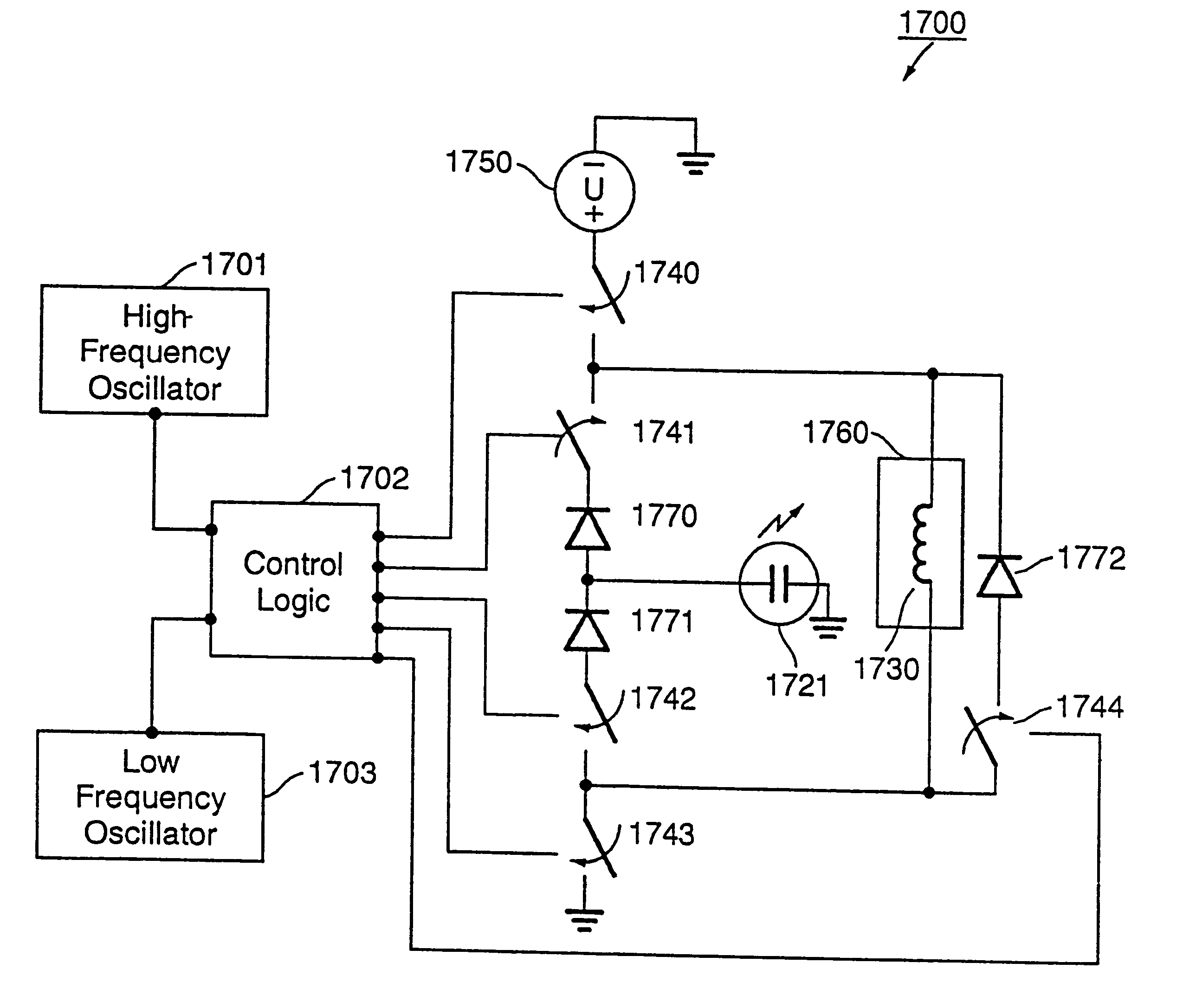
A driver circuit 1000 for driving functional devices, such as an LED 1020-1023, a buzzer 1060, a voltage converter or an EL-lamp, and a method of operating the driver circuit are provided. The circuit includes an inductor 1030, first and second connection points for connection of a voltage source 1050, switching means 1040 which when in a first state allows an electrical current to flow from the first connection point and through the inductor to thereby charge the inductor with energy and when in a second state substantially prevents an electrical current from flowing from the first connection point to the inductor and at least two functional devices, the function of which are activated when energy is discharged from the inductor to the at least two functional devices.

Description

TECHNICAL FIELD OF THE INVENTIONThe present invention refers to a driver circuit having an inductor, first and second connection points for connection of a voltage source, switching means which when in a first state allows an electrical current to flow from the first connection point and through the inductor to thereby charge the inductor with energy and when in a second state substantially prevents an electrical current from flowing from the first connection point to the inductor. It also refers to a method of operating the same.DESCRIPTION OF THE PRIOR ARTDrivers for Light Emitting Diodes, LED's, are well known in the prior art.A first type of LED driver comprises a resistor, an LED and a switch connected to a voltage source. A first electrode of the resistor is connected to the anode of the LED. The cathode of the LED is connected to a first electrode of the switch. The electrode of the voltage source having the most positive potential, "plus-pole", is connected to the second ele...

Claims


Application Information

Patent Timeline
IPC IPC(8): H05B33/02H05B33/08G10K9/12G10K15/04H02M3/155H03K17/00H05B45/37
CPCH05B33/0818H05B45/3725H05B45/375H05B45/38G09F9/00
Inventor ANDERSSON, H.ANG.KANUGGMARK, JOHAN
Owner TELEFON AB LM ERICSSON (PUBL)
Learn More