Probe with tip having micro aperture for detecting or irradiating light, near-field optical microscope, recording/reproduction apparatus, and exposure apparatus using the probe, and method of manufacturing the probe

Inactive Publication Date: 2001-03-13
CANON KK
View PDF11 Cites 92 Cited by
  • Summary
  • Abstract
  • Description
  • Claims
  • Application Information

AI Technical Summary

Problems solved by technology

However, of the above-mentioned prior arts, when the optical probe has no micro aperture like in the PSTM, stray light other than evanescent light such as light scattered by the three-dimensional pattern on the sample surface is detected, thus dropping the resolution.
On the other hand, the prior arts shown in FIGS. 14A and 14B have poor productivity and can hardly attain integration and size reduction of the micro aperture since they present micro aperture formation processes for only one fiber probe.
Also, high cost is required due to complicated, time-consuming processes.
Furthermore, it is hard to strictly control the diameter of the micro aperture, resulting in poor reproducibility.
However, positioning control of such apparatus is complicated, and variations are readily produced.
Moreover, since such working method must be done for each point, the yield is poor.

Method used


Image

  • Probe with tip having micro aperture for detecting or irradiating light, near-field optical microscope, recording/reproduction apparatus, and exposure apparatus using the probe, and method of manufacturing the probe
  • Probe with tip having micro aperture for detecting or irradiating light, near-field optical microscope, recording/reproduction apparatus, and exposure apparatus using the probe, and method of manufacturing the probe
  • Probe with tip having micro aperture for detecting or irradiating light, near-field optical microscope, recording/reproduction apparatus, and exposure apparatus using the probe, and method of manufacturing the probe

Examples


first embodiment

[First Embodiment]

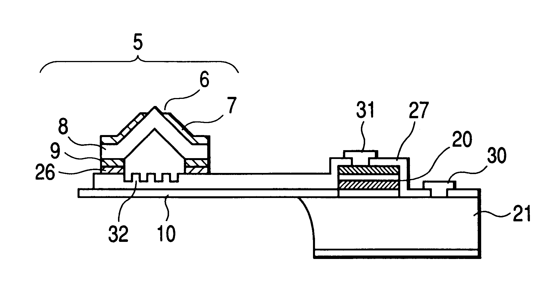
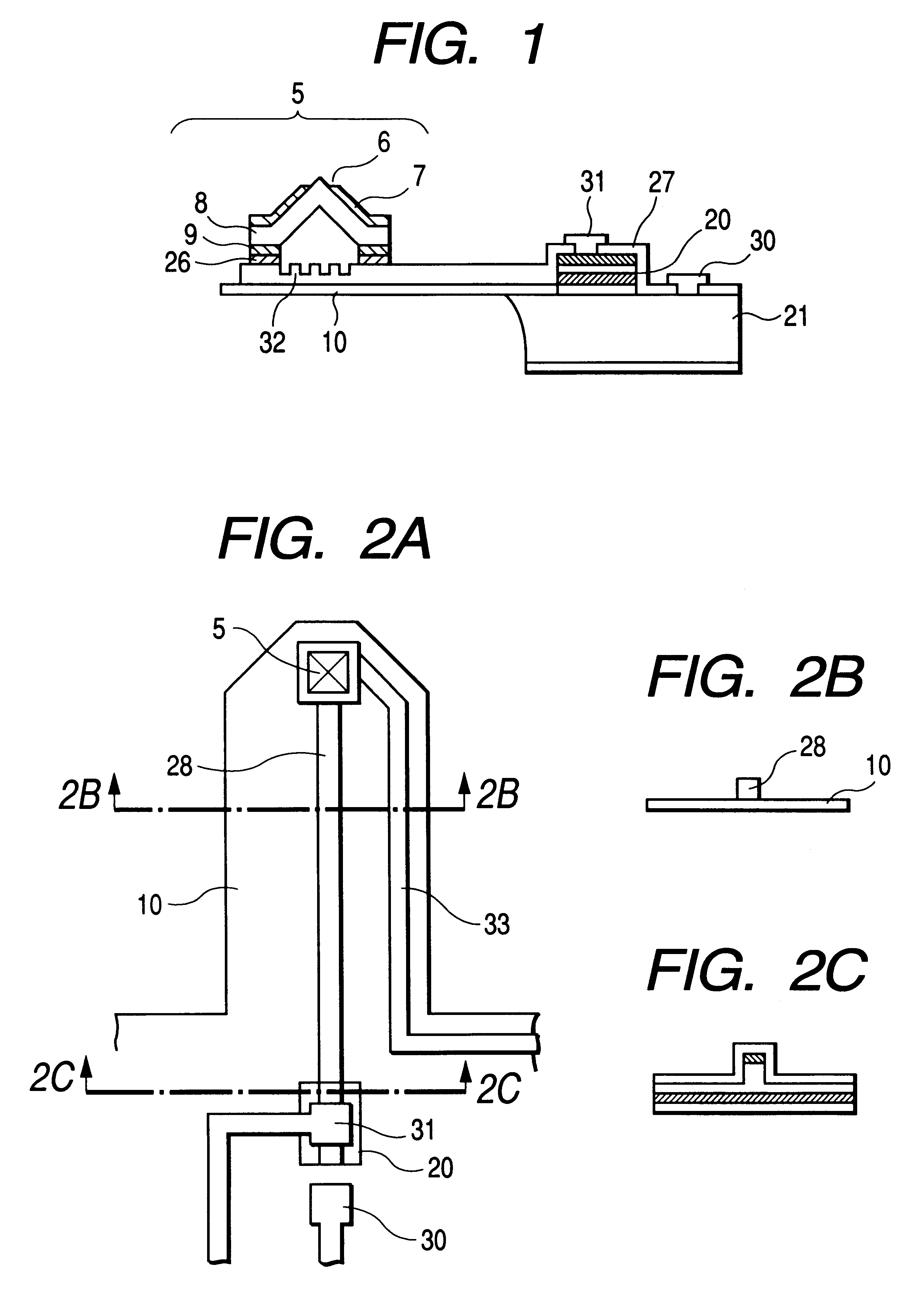
The first embodiment is directed to an evanescent light probe and its manufacturing method according to the present invention. FIGS. 1 and 2A to 2C show the structure of the probe.

The probe of this embodiment comprises an elastic lever 10 formed on a substrate 21, a tip 5 which is formed on the free end portion of the elastic lever and irradiates evanescent light, a laser 20, and a waveguide 28 for optically connecting the laser 20 and the tip 5.

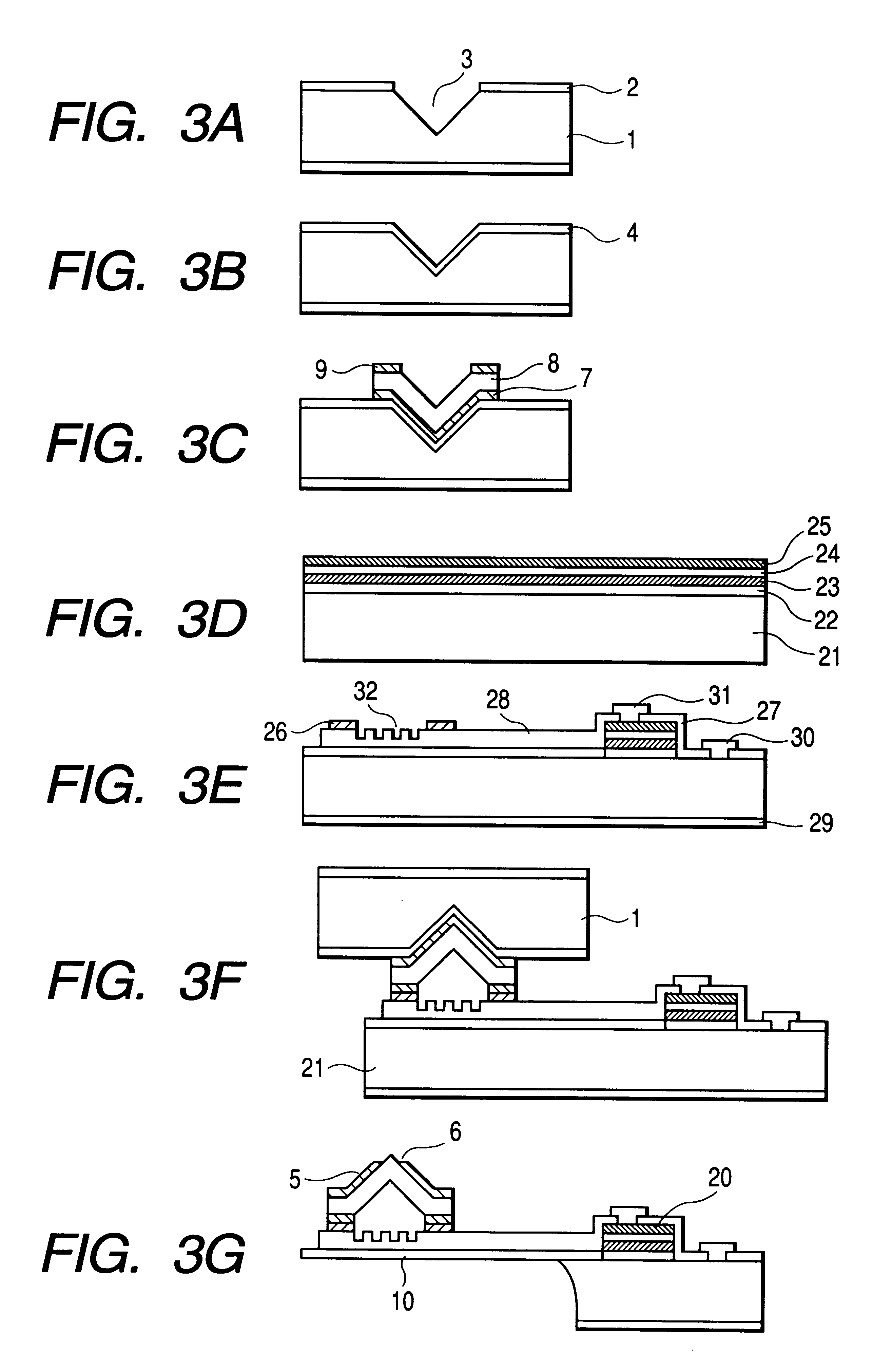
FIGS. 3A to 3G are sectional views showing the manufacturing processes of the evanescent light probe according to this embodiment.

The manufacturing method will be explained below with reference to FIGS. 3A to 3G.

A (100) single-crystal silicon wafer was prepared as a first substrate 1.

A 100-nm thick silicon thermal oxide film was formed as a protection layer 2. A desired portion of the protection layer 2 was patterned by photolithography and etching to expose 10-.mu.m.sup.2 silicon.

The silicon exposed from the patterned port...

second embodiment

[Second Embodiment]

The second embodiment is directed to another evanescent light probe and its manufacturing method according to the present invention.

FIG. 5 shows the structure of the probe. The probe of this embodiment comprises an elastic lever 10 formed on a substrate 21, a tip 5 which is formed on the free end portion of the elastic lever and detects evanescent light, a light-receiving element 19, and a waveguide 28 for optically connecting the light-receiving element 19 and the tip 5.

The light-receiving element 19 has the same structure as that of the laser 20 used in the first embodiment, and when a reverse electric field is applied, carriers are excited and a current flows in response to incoming light. In this way, evanescent light can be detected. In this embodiment, a plurality of probes are disposed on the second substrate 21.

FIGS. 6A to 6G are sectional views showing the manufacturing processes of the evanescent light probe according to this embodiment.

The manufacturing...

third embodiment

[Third Embodiment]

The third embodiment is directed to still another evanescent light probe and its manufacturing method according to the present invention. FIGS. 8, 9A and 9B show the structure of the probe.

The probe of this embodiment comprises an elastic lever 10 formed on a substrate 21, an evanescent light tip 5 formed on the free end portion of the elastic lever, a light-receiving element 19, a laser 20, and a waveguide 28 for optically connecting the light-receiving element 19 and laser 20 to the tip 5.

When the laser 20 used in the first embodiment and the light-receiving element 19 used in the second embodiment are connected to the tip (tip), return light of evanescent light irradiated from the tip onto a recording medium 18 can be detected. In this embodiment, a plurality of probes are disposed on the second substrate 21.

FIGS. 10A to 10G are sectional views showing the manufacturing processes of the evanescent light probe according to this embodiment.

The manufacturing method...


PUM


Abstract

A probe for detecting or irradiating light includes a displaceable support member on a substrate, a tip formed on the support member, and a bonding layer for bonding the tip onto the support member. The tip has a micro aperture. When a light-shielding layer is further formed on a surface of the tip, the micro aperture is formed on the light-shielding layer. The tip consists of a light transmission material.

Description

1. Field of the InventionThe present invention relates to a probe having a tip (stylus) with a micro aperture for detecting or irradiating evanescent light and used in, e.g., a near-field optical microscope or the like, a near-field optical microscope, recording / reproduction apparatus, and exposure apparatus using the probe, and a method of manufacturing the probe.2. Related Background ArtRecently, since the development of a scanning tunneling microscope (to be abbreviated as an "STM" hereinafter) that can directly observe the electron structure of surface atoms of a conductor (G. Binnig et al., Phys. Rev. Lett, 49, 57 (1982)) to allow high-resolution measurement of real space images irrespective of single crystal and amorphous, a scanning probe microscope (to be abbreviated as an "SPM" hereinafter) has been enthusiastically studied in the field of microstructural evaluation of materials.As an SPM, a scanning tunneling microscope (STM), atomic force microscope (AFM), magnetic force ...

Claims


Application Information

Patent Timeline
IPC IPC(8): G03F7/20G11B7/22G12B21/06G12B21/00G11B7/12G01N37/00G01B11/30G01Q20/02G01Q60/22G01Q60/36G01Q70/14G02B21/00G02B27/40
CPCB82Y20/00B82Y35/00G01Q60/22G03F7/70375G03F7/70616G11B7/1203G11B7/22G01Q80/00Y10S977/875Y10S977/862G11B7/122
Inventor SHIMADA, YASUHIROKURODA, RYO
Owner CANON KK
Why Eureka
Try Eureka