Semiconductor device and method for making the same
Inactive Publication Date: 2001-03-20
ROHM CO LTD
View PDF12 Cites 65 Cited by
Summary
Abstract
Description
Claims
Application Information
AI Technical Summary
This helps you quickly interpret patents by identifying the three key elements:
Problems solved by technology
Method used
Benefits of technology
Benefits of technology
It is therefore an object of the present invention to provide a semiconductor device wherein a package of the semiconductor device has a lower surface formed with a plurality of external terminal portions arranged in a matrix pattern, and wherein the thickness and weight of the package can be further reduced.
As already described for the second aspect of the present invention, by using the above frame, the manufacture of the semiconductor device having a basic arrangement in which the semiconductor chip is bonded to the upper surface of the film substrate can be performed efficiently without troubles.
Problems solved by technology
However, the conventional semiconductor device described above has following problems since the semiconductor chip is mounted to the insulated substrate which is rigid and is made of glass epoxy resin.
First, the thickness of the rigid substrate takes up a considerable part of the total thickness of the semiconductor device.
This limits further miniaturization of the semiconductor device in terms of the thickness as well as limiting further reduction in weight.
Second, the rigid substrate made of glass epoxy resin has a coefficient of thermal expansion which is very different from that of the semiconductor chip.
Thus, when the semiconductor device is being mounted to the mother substrate, heat applied during the operation may cause excessively large differences in expansion, destroying mechanical or electrical connection between the semiconductor chip and the insulated substrate.
Third, since the rigid substrate has a considerable thickness, it is difficult to further increase disposition density of the external terminal portions formed in the lower surface of the rigid substrate.
This limits the disposition density of the external terminal portions, limiting the number of usable terminals in the semiconductor chip for making the semiconductor device, making it impossible to appropriately meet the demand for high-density mounting, as well as making manufacture more costly due to a large consumption of solder.
Method used
Image
Click on the blue label to locate the original text in one second.
Reading with bidirectional positioning of images and text.
Examples
first embodiment
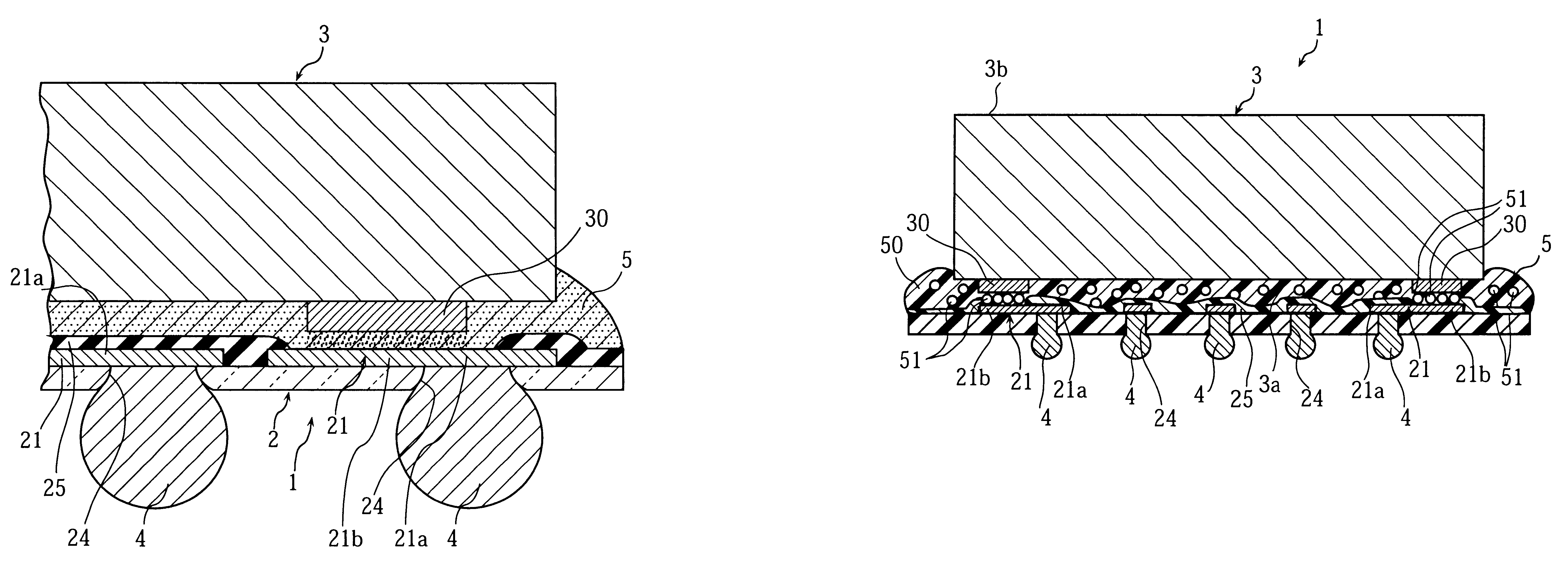
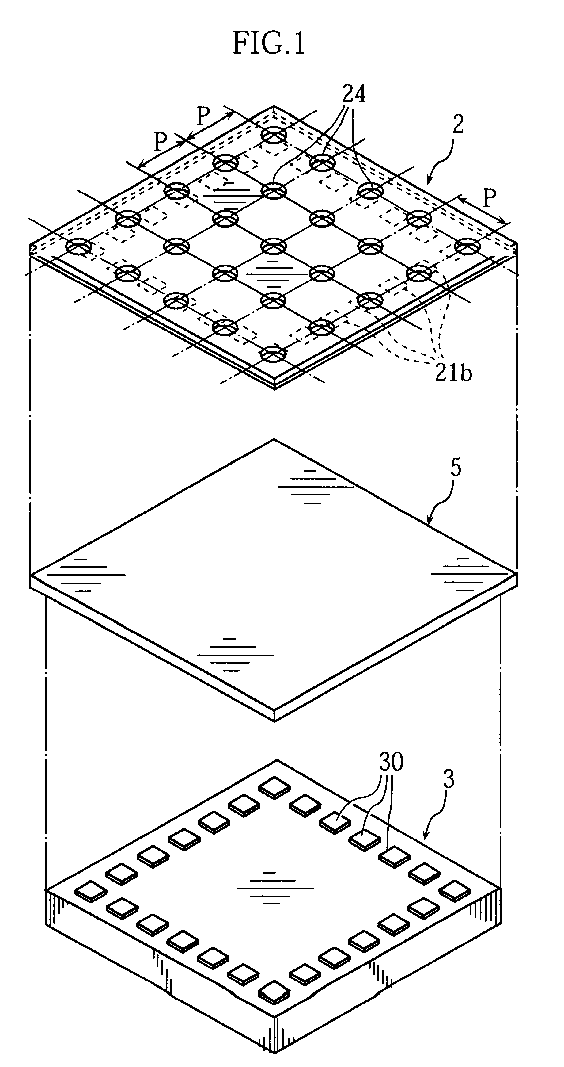
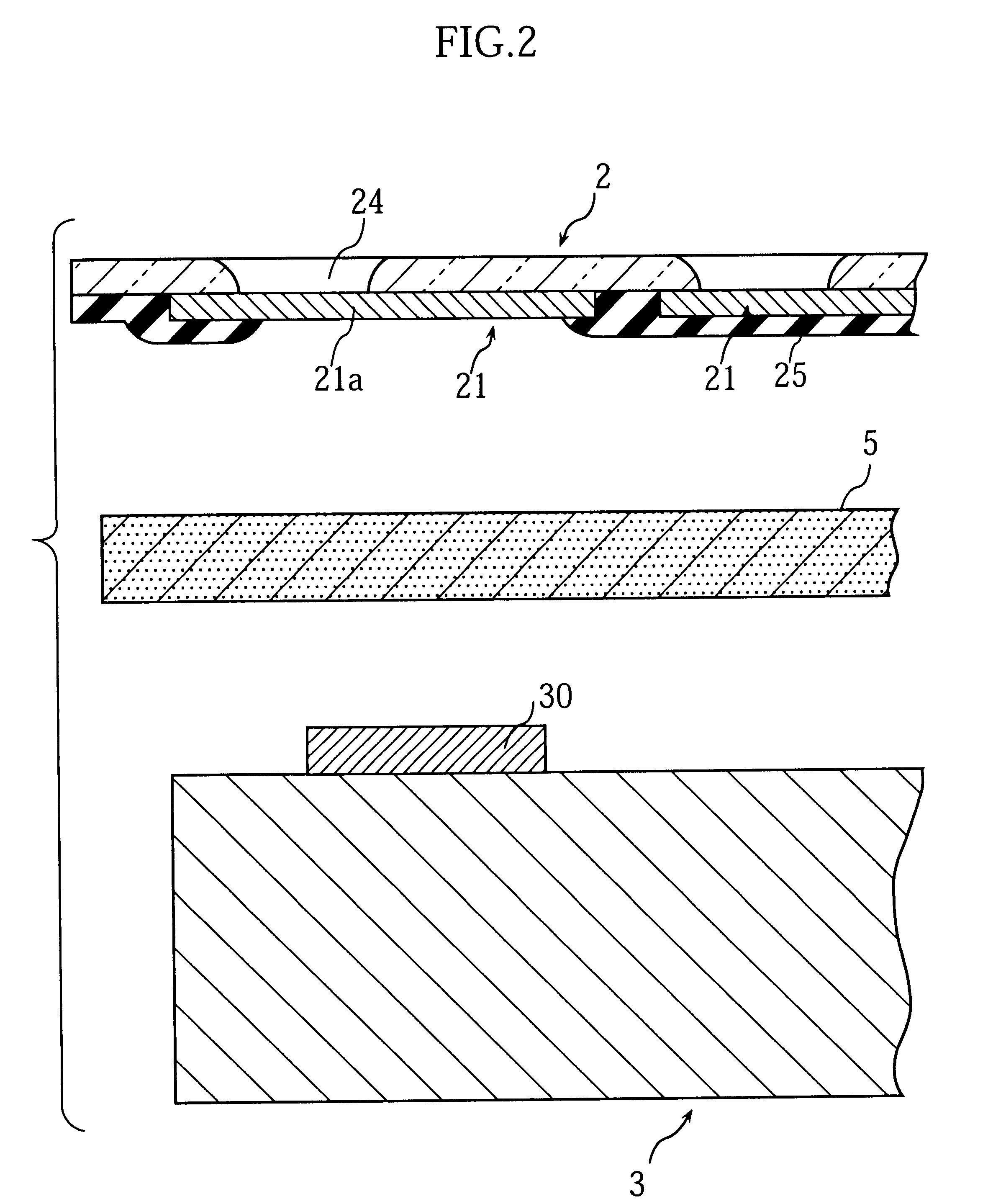
First, reference will be made to FIGS. 1 through 6, and a semiconductor device 1 as the present invention will be described.
This semiconductor device 1 comprises a film substrate 2 and a semiconductor chip 3 mounted to an upper surface of the film substrate 2. The semiconductor chip 3 is mounted in a "face down" manner.
The film substrate 2 is primarily made of a polyimide resin film having a thickness of a few tens of micron meters for example. The upper surface of the film substrate 2 is formed with a plurality of wiring patterns 21 made of a foil of metal such as copper or gold. A lower surface of the film substrate 2 is formed with a plurality of external terminal portions 4 disposed in a matrix pattern. The external terminal portions 4 are spaced from each other by a pitch P both laterally and longitudinally, and electrically connected respectively with the wiring patterns 21.
More specifically, the film substrate 2 is formed with the plurality of holes 24 of a predetermined size...
second embodiment
Next, reference will be made to FIGS. 7 through 15, and description will be made for a semiconductor device 1 as the present invention.
As shown in FIGS. 7 through 9, the semiconductor device 1 according to this embodiment also comprises a film substrate 2 mounted with a semiconductor chip 3. The film substrate 2 and the semiconductor chip 3 are mechanically and electrically connected to each other via an anisotropic conductive adhesive 5 placed in between. The semiconductor chip 3 has side surfaces 3c surrounded by a protective resin 6. The film substrate 2 has a matrix of external terminal portions 4 projecting out of the lower surface of the film substrate 2.
The semiconductor chip 3 is a bear chip such as an IC chip or an LSI chip, including a main surface 3a having circumferential edges along which a plurality of electrode pads 30 are formed. Similarly to the previous embodiment, these electrode pads 30 are formed as bump terminals. Specifically for example, the main surface 3a o...
third embodiment
Next, reference is made to FIGS. 16 through 18 to see the present invention.
A semiconductor device 1 according to this embodiment is similar to the semiconductor device 1 according to the second embodiment shown in FIGS. 7 through 9. However, the protective resin which surrounds the semiconductor chip 3 is not used in the semiconductor device 1 in this third embodiment. Further, according to the present embodiment, each of wiring patterns 21 formed in an upper surface of a film substrate 2 has an end portion 21a extended inwardly of a corresponding terminal pad 30 of a semiconductor chip 3 as viewed from above, into a region inward of the terminal pads 30. Except these differences, all the other arrangements are practically the same as the second embodiment, and therefore corresponding members and portions are identified by the same alpha-numeral code, and no further description will be made. Further, the semiconductor device 1 according to this third embodiment can be manufactured ...
PUM
Abstract
A semiconductor device comprising a film substrate and a semiconductorchip bonded to an upper surface of the film substrate is provided. The semiconductorchip has a main surface formed with a plurality of terminal pads. The film substrate has a lower surface formed with a plurality of external terminal portions in a matrix pattern, and an upper surface formed with a plurality of wiring patterns for respectively connecting with the external terminal portions. The wiring patterns formed in the upper surface of the film substrate are respectively connected to the terminal pads formed on the main surface of the semiconductor chip.
Description
1. Field of the InventionThe present invention relates to a semiconductor device and a method for making the same. More specifically, the present invention relates to a semiconductor device formed into a small package having a lower surface formed with a plurality of external terminal portions arranged in a matrix pattern, and a method of making such a semiconductor device.2. Background ArtA semiconductor device commonly called BGA (Ball Grid Array) package type or area array package type comprises an insulated substrate having a lower surface formed with a plurality of external terminal portions arranged in a matrix pattern. On an upper surface of this substrate, a semiconductor chip is mounted. Conventionally, the insulated substrate is a rigid substrate typically made of a glass epoxy resin. This rigid substrate has a lower surface formed with a plurality of external terminal portions typically made of solder arranged in a matrix pattern. On the other hand, an upper surface of th...
Claims
Application Information
Patent Timeline
Application Date:The date an application was filed.
Publication Date:The date a patent or application was officially published.
First Publication Date:The earliest publication date of a patent with the same application number.
Issue Date:Publication date of the patent grant document.
PCT Entry Date:The Entry date of PCT National Phase.
Estimated Expiry Date:The statutory expiry date of a patent right according to the Patent Law, and it is the longest term of protection that the patent right can achieve without the termination of the patent right due to other reasons(Term extension factor has been taken into account ).
Invalid Date:Actual expiry date is based on effective date or publication date of legal transaction data of invalid patent.

