Forming contacts on semiconductor substrates, radiation detectors and imaging devices

a technology of semiconductor substrates and contacts, applied in the direction of x/gamma/cosmic radiation measurement, radiation controlled devices, instruments, etc., can solve the problems of poor electrical separation of individual contacts, which results from the conventional method of forming such contacts, and achieves stable performance, reduce inter-contact resistivity, and increase surface leakage current

Inactive Publication Date: 2001-04-10
SIEMENS HEALTHCARE GMBH
View PDF7 Cites 36 Cited by
  • Summary
  • Abstract
  • Description
  • Claims
  • Application Information

AI Technical Summary

Benefits of technology

The present inventors have found that the surface resistivity of a CdZnTe semiconductor substrate is degraded when the substrate is exposed to metal etchants suitable for removing gold and / or platinum. As a result, the electrical separation of the individual contacts which result from the conventional method of forming such contacts is not as good as would be expected from the properties of that material before treatment. By using a method in accordance with the present invention, the surface of the semiconductor substrate between the contacts can be isolated from the metal etchants, thus preventing the damage which would result if the metal etchants came into contact with the semiconductor surface.
Alternatively, this step may include the sub-steps of forming a layer of passivation material on the substrate surface; forming a layer of photoresistive material on the passivation layer; selectively exposing the photoresistive material, and removing the photoresistive material from areas corresponding to the contact positions to expose the passivation material layer; and removing the passivation material from the exposed areas corresponding to the contact positions to expose the substrate surface. The use of an insulating layer of passivation material means that after manufacture of the detector, the passivation material remains between the contacts, protecting the semiconductor surface from environmental damage in use and further enhancing the electrical separation of the contacts. To protect the other main surface and the sides (edges) of the semiconductor substrate, photoresistive material can additionally be applied to all exposed surfaces prior to the step of removing the passivation material from the exposed areas corresponding to the contact positions.
Again with reference to the above-referenced first embodiment, the step of removing metal overlying the layers of material to separate individual contacts may include the steps of forming a further layer of photoresistive material on at least the metal layer; selectively exposing the photoresistive material of the further layer, and removing the photoresistive material of the further layer apart from areas corresponding generally to the openings; and removing metal not covered by the photoresistive material of the further layer. In addition, any remaining photoresistive material may be removed. In a variation on this embodiment, the areas corresponding generally to the openings are larger than the corresponding openings, so that after removal of the metal not covered by the photoresistive material of the further layer, the contacts cover the opening and also extend up and laterally beyond the opening. In this way the ingress of metal etchant around the photoresistive material, whereby the metal etchant might reach the semiconductor surface, can be avoided.
Another embodiment of the present invention provides a method of manufacturing, for example, detectors having a CdZnTe substrate with one side uniformly metallized with gold and the other side patterned with gold structures in a manner that does not adversely affect the surface characteristics of the CdZnTe substrate between the gold structures. Using such a method, it is possible to create gold structures on one side of a CdZnTe detector and achieve inter-structure resistivity on the order of G.OMEGA. / square (or tens or hundreds of G.OMEGA. / square).
The use of an electrically-insulating passivation layer between contacts further enables the area between metal contacts to be protected, thus giving a detector according to an embodiment of the present invention stable performance over time and avoiding effects such as oxidation which increase the surface leakage current and decrease the inter-contact resistivity. Aluminum nitride (AlN) passivation has been found to be particularly effective when applied between gold contacts to protect the surface and enhance the electrical separation of the gold contacts. The passivation layer of aluminum nitride can be implemented at relatively low temperatures, typically less than 100.degree. C. By contrast, silicon oxide (SiO.sub.2), which is typically used as a passivant for silicon (Si) semiconductors, needs temperatures in excess of 200.degree. C. CdZnTe would be unusable after exposure to such temperatures.

Problems solved by technology

As a result, the electrical separation of the individual contacts which result from the conventional method of forming such contacts is not as good as would be expected from the properties of that material before treatment.

Method used


Image

  • Forming contacts on semiconductor substrates, radiation detectors and imaging devices
  • Forming contacts on semiconductor substrates, radiation detectors and imaging devices
  • Forming contacts on semiconductor substrates, radiation detectors and imaging devices

Examples


Embodiment Construction

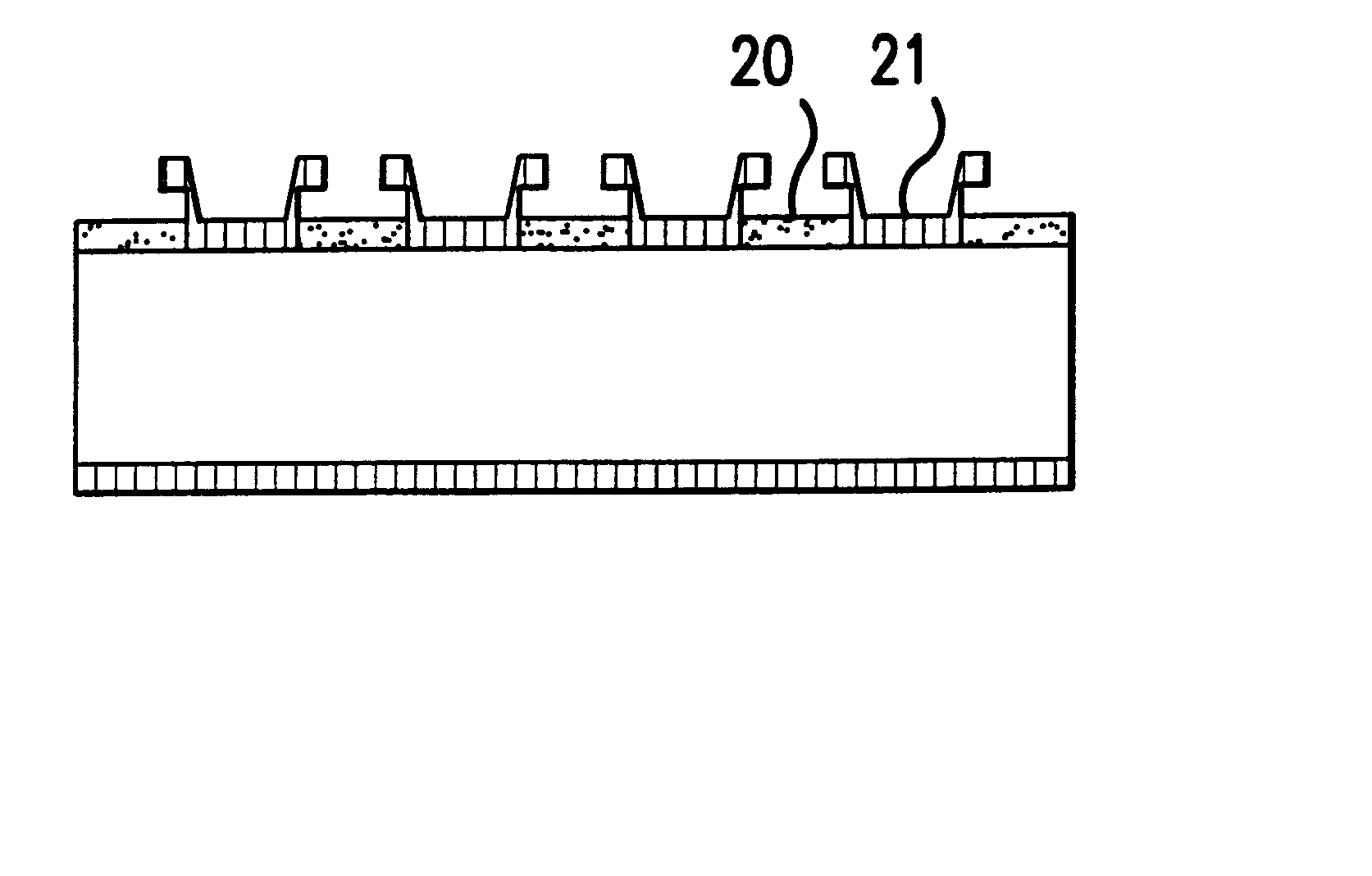
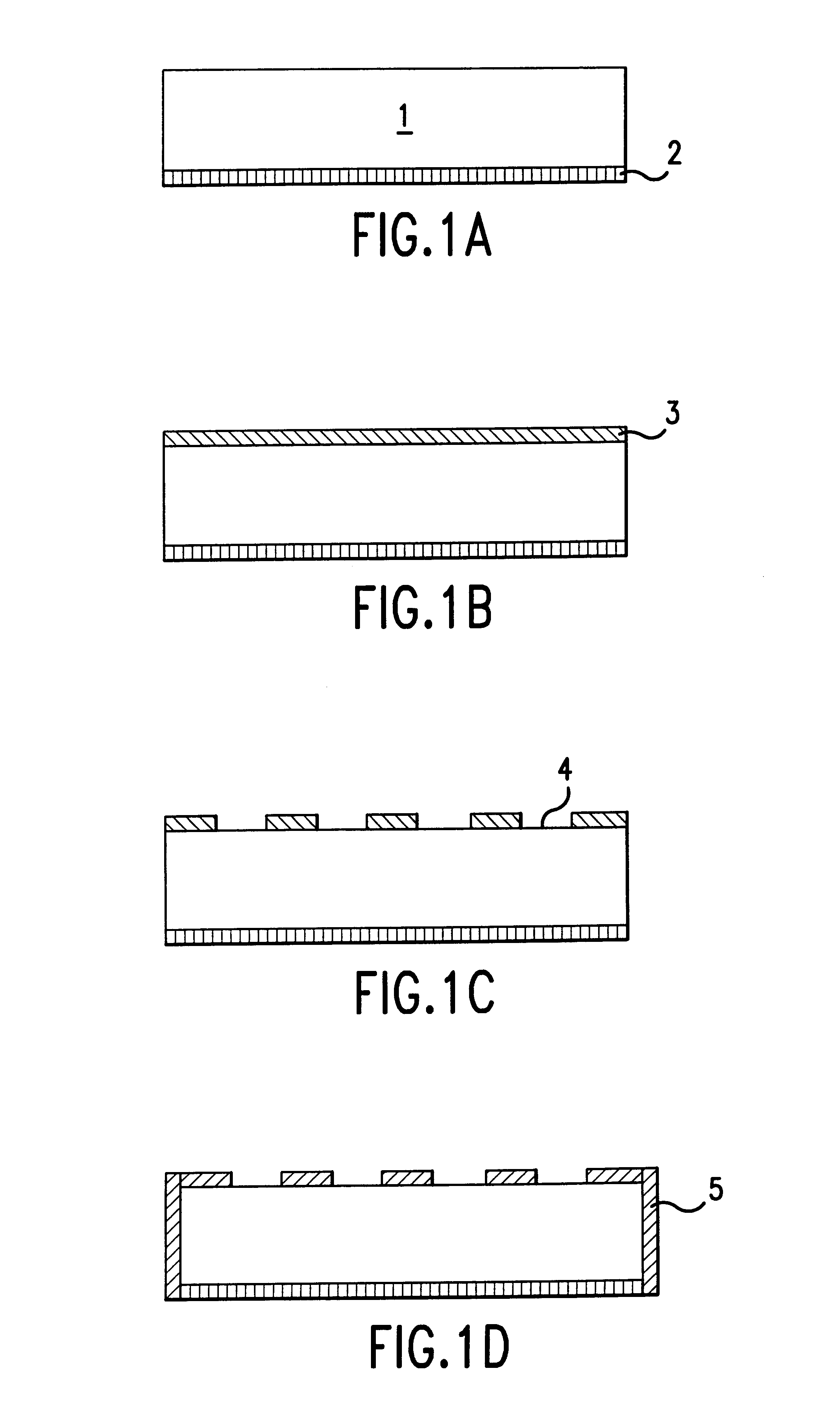
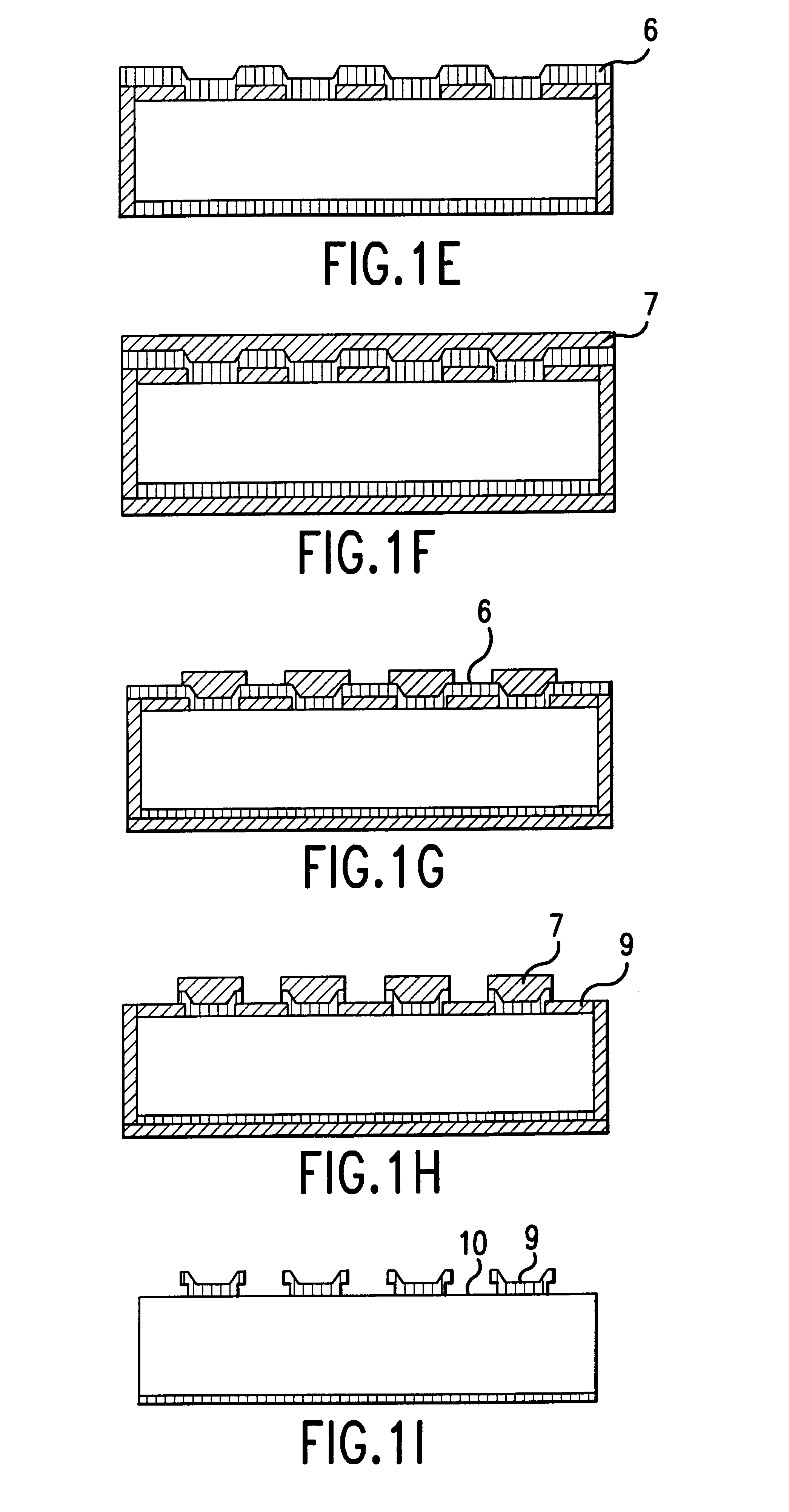
FIGS. 1A-1I illustrate in progressive fashion a method for forming metal contacts on a semiconductor substrate at positions for defining radiation detector cells, according to an embodiment of the present invention. The series of drawings presents schematic cross-sectional views from the side of a detector at various stages in the formation of metal contacts on a semiconductor substrate. In this embodiment, the semiconductor substrate is made of cadmium zinc telluride (CdZnTe), although other semiconductor materials, such as cadmium telluride (CdTe), may also be used. Likewise, the metal used for the metallization layer and the metal contacts is gold, although other metals, alloys or conductive materials, including platinum and indium, may also be used.

In the following description, various method steps are described with reference to a corresponding one of the series of FIGS. 1A-1I. For example, "Step A" corresponds to FIG. 1A, "Step B" corresponds to FIG. 1B, and so on.

Step A

A dete...


PUM


Abstract

A method, suitable for forming metal contacts on a semiconductor substrate at positions for defining radiation detector cells, includes the steps of forming one or more layers of material on a surface of the substrate with openings to the substrate surface at the contact positions; forming a layer of metal over the layer(s) of material and the openings; and removing metal overlying the layer(s) of material to separate individual contacts. Optionally, a passivation layer to be left between individual contacts on the substrate surface may be applied. Etchants used for removing unwanted gold (or other contact matter) are preferably prevented from coming into contact with the surface of the substrate, thereby avoiding degradation of the resistive properties of the substrate.

Description

BACKGROUND OF THE INVENTION1. Field of the InventionThe invention relates to methods for manufacturing radiation detectors and radiation imaging devices, radiation detectors and imaging devices manufactured by such methods, and the use of such radiation detectors and imaging devices.2. Description of the Prior ArtA typical method of manufacturing a radiation detector for an imaging device comprises applying a layer of a metal such as aluminum to both of the main surfaces of a planar semiconductor substrate, applying a layer of photoresistive material to cover the semiconductor material, exposing the photoresistive material on the surface of the planar substrate with an appropriate mask pattern, removing the photoresistive material to expose a pattern of the metal to be removed, etching away the metal to be removed, and then removing the remaining photoresistive material to leave a pattern of contacts on one surface of the substrate and a metallized layer on the other surface of the ...

Claims


Application Information

Patent Timeline
Patent Type & Authority Patents(United States)
IPC IPC(8): H01L21/70H01L21/8234H01L27/146H01L21/28G01T1/24H01L27/14H01L31/0224H01L31/0264
CPCH01L21/823406H01L27/14643H01L31/022408Y10S438/958Y10S438/93
Inventor ORAVA, RISTO O.PYYHTIA, JOUNI I.SCHULMAN, TOM G.SARAKINOS, MILTIADIS E.SPARTIOTIS, KONSTANTINOS E.JALAS, PANU Y.
Owner SIEMENS HEALTHCARE GMBH
Why Eureka
Try Eureka