Method and apparatus for the optimization of a tree depth for clock distribution in semiconductor integrated circuits

a technology of integrated circuits and tree networks, applied in the field of distribution, can solve the problems of inapplicability of prior art, delay in clock signal receiving by elements, and lack of consideration of power consumption of h-tree networks

Inactive Publication Date: 2001-05-08
KK TOSHIBA
View PDF4 Cites 34 Cited by
  • Summary
  • Abstract
  • Description
  • Claims
  • Application Information

AI Technical Summary

Benefits of technology

Another object of the present invention is to provide a method and apparatus for speedily calculating the optimum depth of a tree network for distributing a clock signal to elements of a semiconductor integrated circuit without a knowledge of skilled designers, thereby reducing the development period and manufacturing cost of semiconductor devices.

Problems solved by technology

Actually, the clock signal received by the elements involves delay due to the resistance and capacitance of the metal lines used to distribute the clock signal to the elements.
However, the prior arts mentioned above give no consideration on power consumption of an H-tree networks.
The objective of this prior art, however, is an H-tree network without multistage buffering, and therefore, the prior art is inapplicable to H-tree networks employing multistage buffering.

Method used


Image

  • Method and apparatus for the optimization of a tree depth for clock distribution in semiconductor integrated circuits
  • Method and apparatus for the optimization of a tree depth for clock distribution in semiconductor integrated circuits
  • Method and apparatus for the optimization of a tree depth for clock distribution in semiconductor integrated circuits

Examples


Embodiment Construction

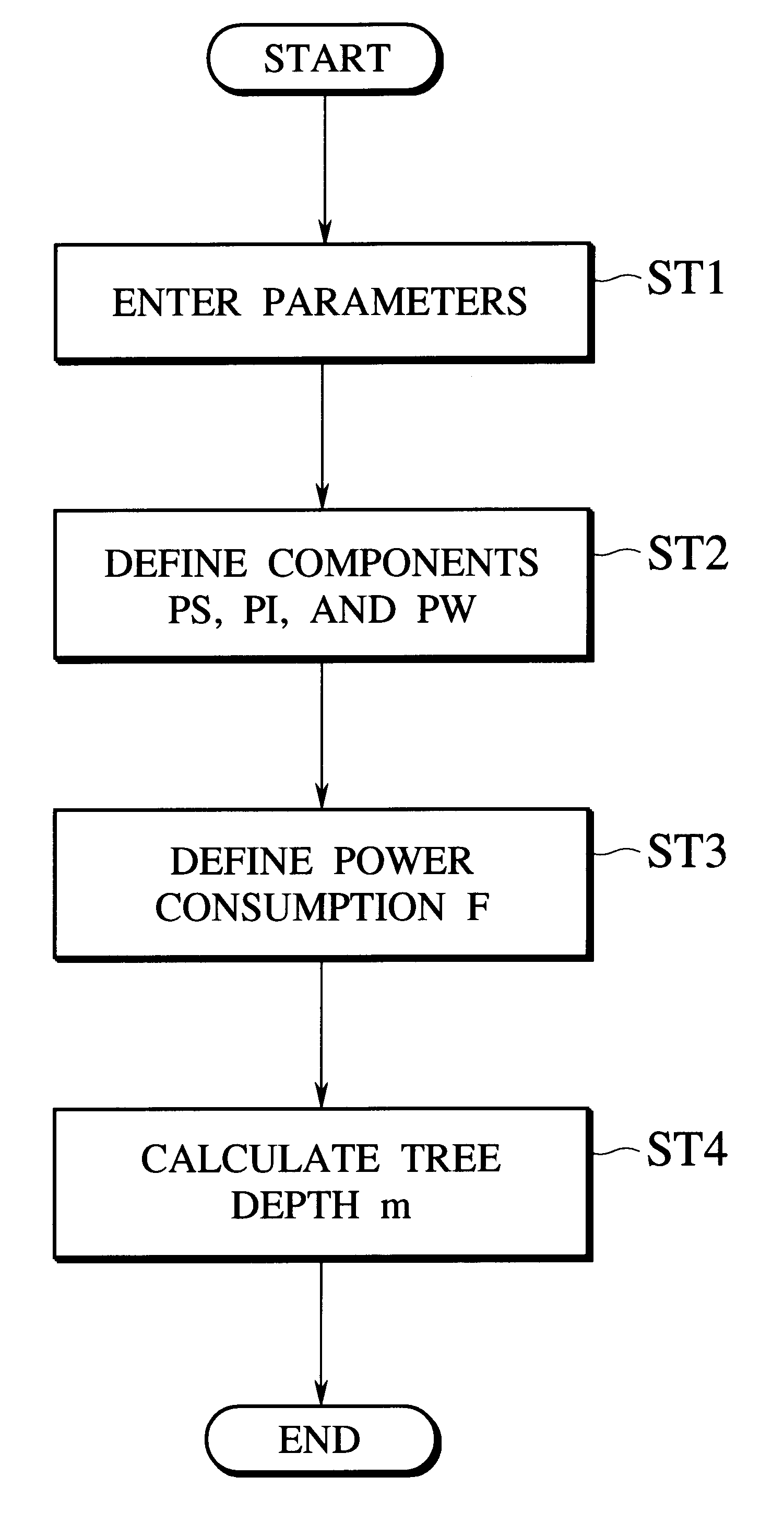
Embodiments of the present invention will be explained with reference to the accompanying drawings.

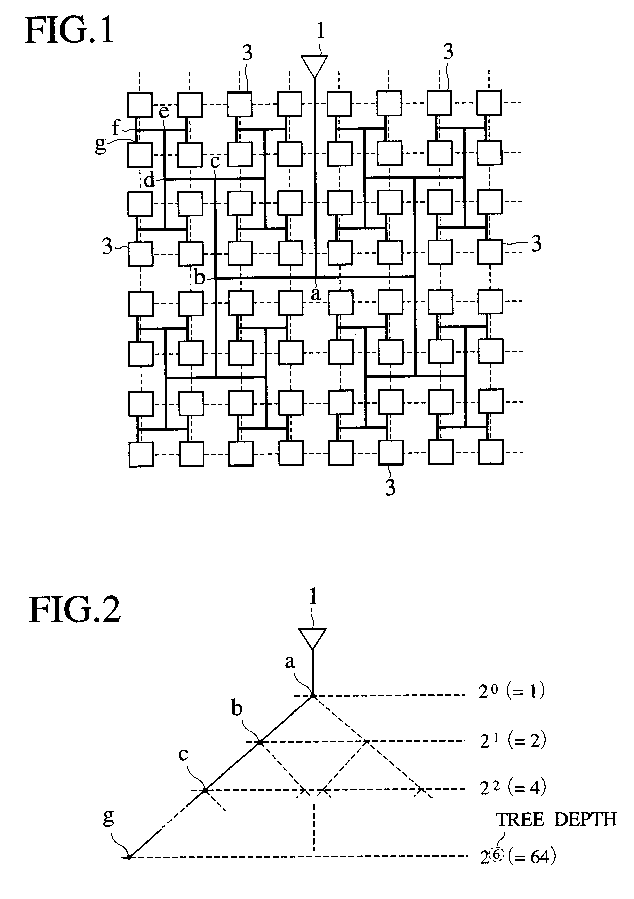
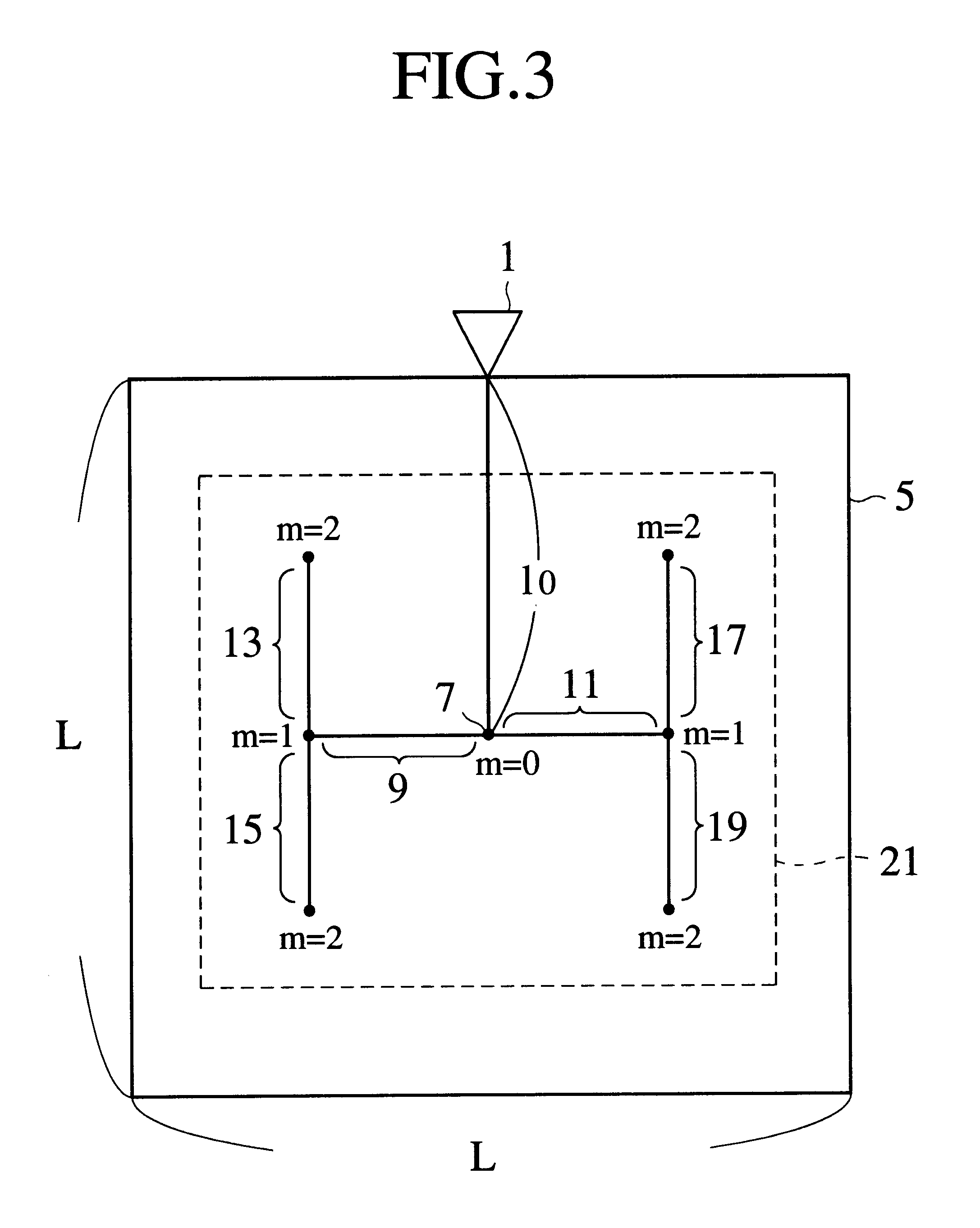
FIG. 1 is a plan view showing an H-tree network for distributing a clock signal to elements of a semiconductor integrated circuit, according to the present invention. This H-tree is called a "completely symmetrized H-tree." The H-tree network is indicated with a thick line and is composed of a repetition of H-shaped wiring. The H-tree network distributes a clock signal from a root driver 1 to all groups 3. Each group 3 contains at least one element, which is a flip-flop in this example. Every wiring segment that connects a pair of the groups 3 has an identical length. Buffer cells are arranged at branching points of the H-tree network. The buffer cells in the last stage of the H-tree network directly distribute the clock signal to the flip-flop groups 3.

Since each H-shaped wiring in the H-tree network is symmetric, the clock signal provides the same delay on every flip-flop group 3.

The...


PUM


Abstract

A method optimizes a tree depth of an H-tree network for distributing a clock signal to elements of a semiconductor integrated circuit, in a way as to minimize power consumption of the H-tree network. The method has the steps of entering parameters, defining a short circuit current component PS, cell internal switching current component PI, and switching current of interconnect capacitance component PW of the power consumption of the H-tree network with equations employing a tree depth m as a variable, defining the power consumption F of the H-tree network as the sum of the components PS, PI, and PW, and finding a tree depth that minimizes the power consumption F. The method differentiates the power consumption F, i.e., the sum of the components PS, PI, and PW with respect to the tree depth m as ∂F / ∂m and solves "∂F / ∂m=0" to find the optimum tree depth of the H-tree network.

Description

1. Field of the InventionThe present invention relates to a technique of distributing a clock signal to elements of a semiconductor integrated circuit, and particularly, to a method and apparatus for optimizing a depth of a tree network for clock distribution with minimal power consumption.2. Description of the Prior ArtImprovements in semiconductor technology have developed large-scale, high-speed semiconductor integrated circuits. These circuits have many elements that must receive clock signals whose frequencies are increasing these days.Synchronous systems realize correct operation timing on elements by synchronizing the operation timing in response to rising edges and falling edges of a clock signal. Ideally, all elements in a semiconductor integrated circuit which need a clock signal must receive it without delay. Actually, the clock signal received by the elements involves delay due to the resistance and capacitance of the metal lines used to distribute the clock signal to th...

Claims


Application Information

Patent Timeline
Patent Type & Authority Patents(United States)
IPC IPC(8): G06F1/10G06F17/50H01L21/822H01L21/82H01L27/04
CPCG06F1/10G06F17/5077G06F2217/78G06F30/394G06F2119/06
Inventor TAKANO, MIDORI
Owner KK TOSHIBA
Why Eureka
Try Eureka