Device for monitoring and calibrating oxide charge measurement equipment and method therefor

a technology of measurement equipment and equipment, which is applied in the direction of individual semiconductor device testing, semiconductor/solid-state device testing/measurement, instruments, etc., can solve the problems of method not meeting accepted quality control standards, inaccurate calibration of oxide charge measurement equipment, and difficult production of calibration wafers

Inactive Publication Date: 2001-06-19
WAFER STANDARDS
View PDF10 Cites 18 Cited by
  • Summary
  • Abstract
  • Description
  • Claims
  • Application Information

AI Technical Summary

Problems solved by technology

There is currently only one common method used for the calibration of mobile ion measurement equipment, and this method is incapable of meeting accepted quality control standards, such as ISO 9000, (International Organization for Standardization (ISO)--Quality management and quality standards assurance.
While the production of calibration wafers, or wafer standards as they are sometimes known, is desirable, these calibration wafers are difficult to produce because the dielectrics of a wafer that have been purposely contaminated with mobile ions tend to be unpredictable and unstable in their use.
The unpredictability and instability of the calibration wafers can result in the incorrect calibration of the oxide charge measurement equipment.
This may then lead to incorrect assessments of the production line equipment and the wafers in process, which in turn leads to faulty or imperfectly operating semiconductor devices.
A further problem is that in order to control the oxide charge in a semiconductor fabrication line, it is necessary to distinguish between the variables associated with the dielectric layer of a wafer under test and the variables in the tester itself.

Method used


Image

  • Device for monitoring and calibrating oxide charge measurement equipment and method therefor
  • Device for monitoring and calibrating oxide charge measurement equipment and method therefor
  • Device for monitoring and calibrating oxide charge measurement equipment and method therefor

Examples


Embodiment Construction

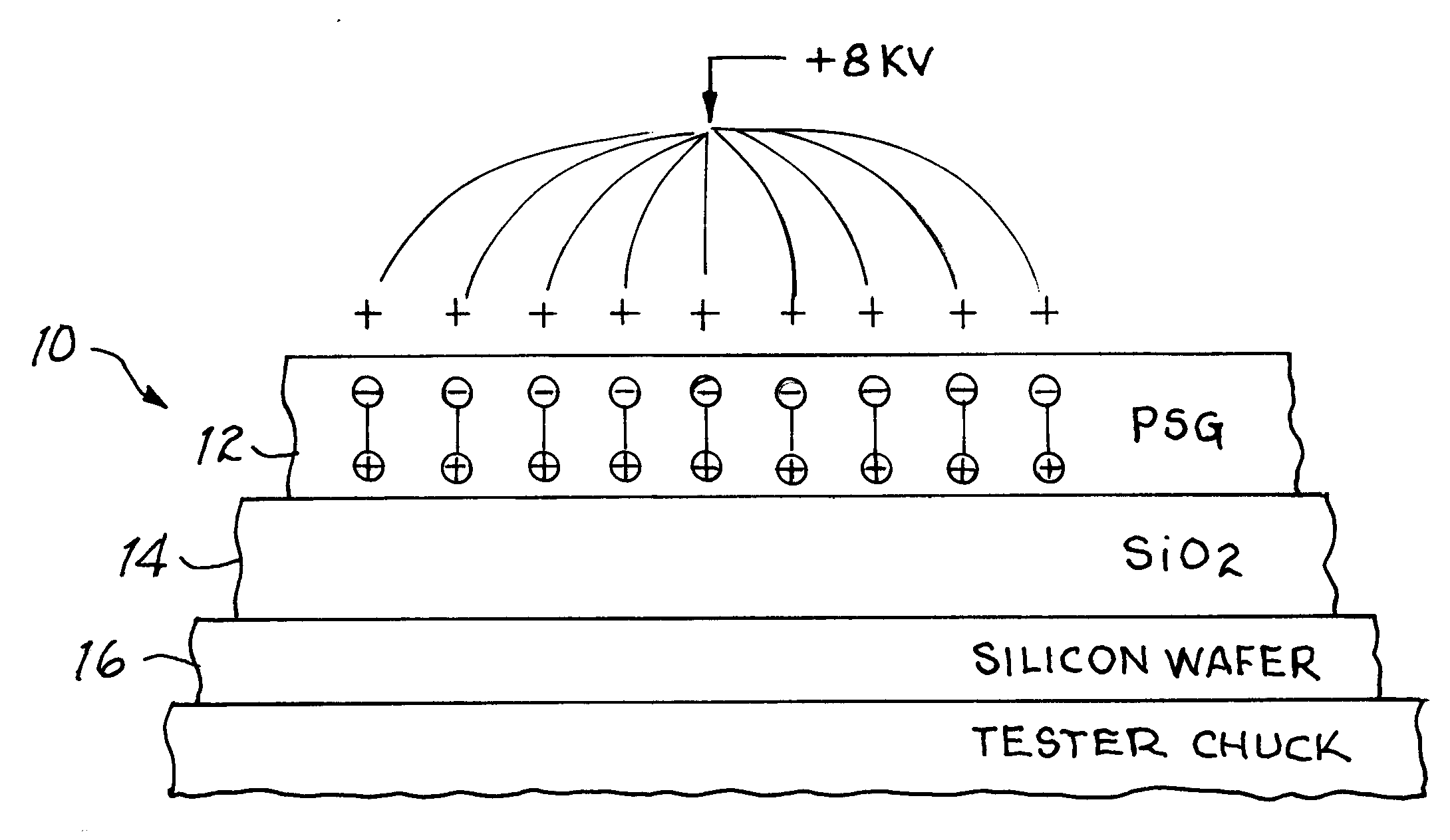
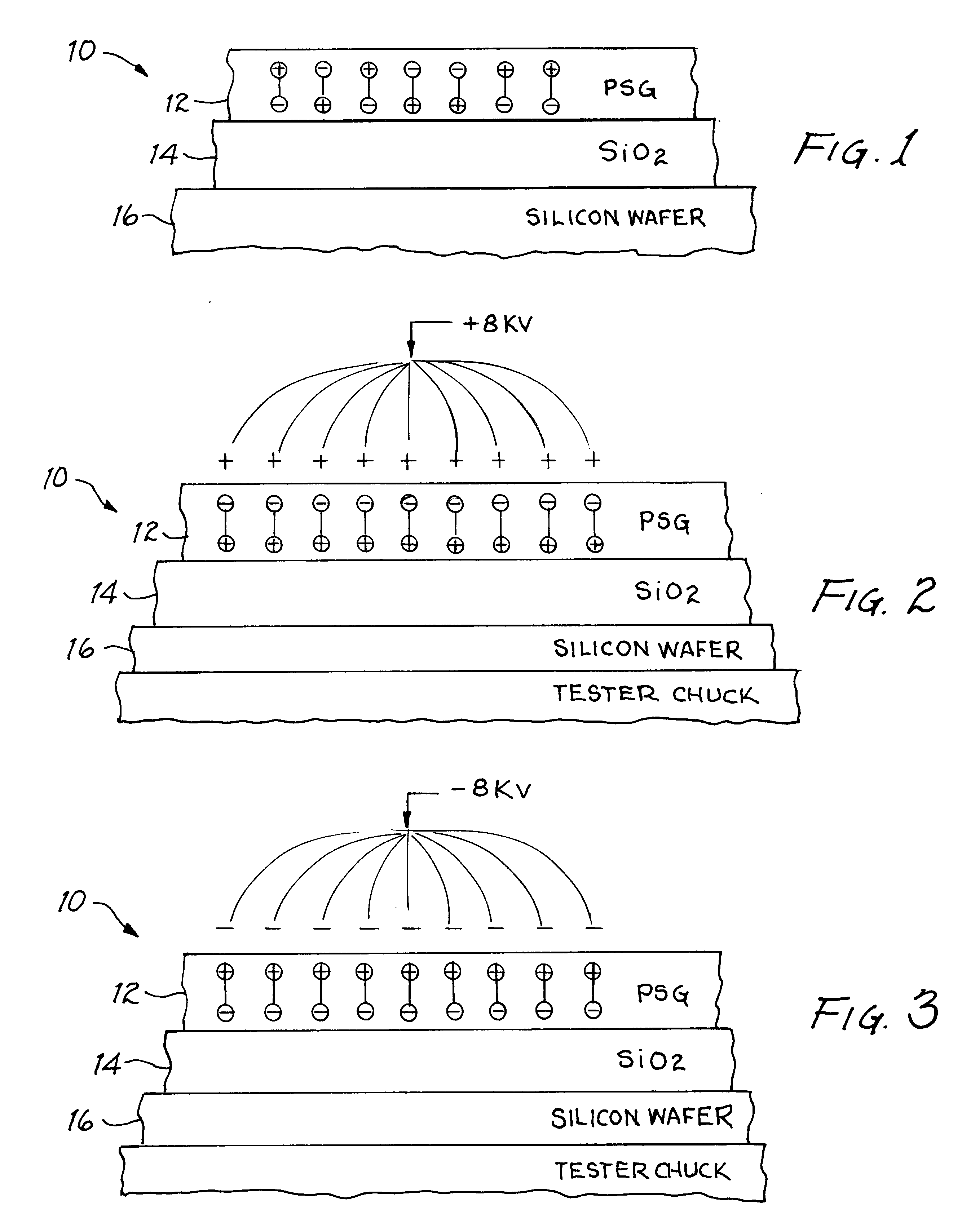
In accordance with a preferred embodiment of the present invention a stabilized wafer for monitoring and calibrating oxide charge test equipment is disclosed. The stabilized wafer for monitoring and calibrating oxide charge test equipment comprises; a silicon wafer, a SiO.sub.2 layer upon the silicon wafer, and a phosphosilicate glass layer formed in the SiO.sub.2 layer for providing the stabilized wafer by stabilizing an SiO.sub.2 interface and containing oxygen ions.

In accordance with another embodiment of the present invention a method of constructing and using a stabilized wafer for monitoring and calibrating oxide charge test equipment is disclosed. The method of constructing and using a stabilized wafer for monitoring and calibrating oxide charge test equipment comprises the steps of; providing a stabilized wafer for stabilizing an SiO.sub.2 interface and containing oxygen ions, and using the stabilized wafer for monitoring and calibrating oxide charge test equipment.

In accord...


PUM


Abstract

A stabilized wafer for monitoring and calibrating oxide charge test equipment. The stabilized wafer comprises; a silicon wafer, a SiO2 layer of at least 100 angstroms upon the silicon wafer, and a phosphosilicate glass layer containing phosphorus formed in the SiO2 layer for providing the stabilized wafer by stabilizing an SiO2 interface and containing oxygen ions. The stabilized wafer is used for monitoring and calibrating oxide charge test equipment.

Description

This invention is in the field of semiconductor fabrication process monitoring and control, and methods therefor, and more particularly, is a device and method that applies to the calibration, monitoring and control of test equipment used on the process line to measure oxide charge including mobile ion contamination.DESCRIPTION OF THE RELATED ARTSemiconductor wafers undergo a variety of measurements to measure and ensure the suitability of the wafer for further processing. Some of these measurements test for acceptable levels of charge time retention, dopant concentration, leakage and mobile ion concentration. In particular, one of these tests, for the detection of mobile ion concentration and other oxide charge is key to the successful fabrication of integrated circuits upon semiconductor wafers in the process line. The monitoring of mobile ion contaminants such as sodium ions or potassium ions is required to ensure that adequate yields result, and also to ensure that the reliabili...

Claims


Application Information

Patent Timeline
Patent Type & Authority Patents(United States)
IPC IPC(8): H01L21/02H01L23/544H01L21/316
CPCH01L21/02129H01L21/022H01L21/02238H01L21/02255H01L21/02321H01L21/02337H01L21/31625H01L22/34H01L2924/0002H01L2924/00
Inventor KOELSCH, RONALD G.KOELSCH, ROBERT
Owner WAFER STANDARDS
Why Eureka
Try Eureka