Multi chip package (MCP) applicable to failure analysis mode

Inactive Publication Date: 2001-07-03
KK TOSHIBA
View PDF8 Cites 40 Cited by
  • Summary
  • Abstract
  • Description
  • Claims
  • Application Information

AI Technical Summary

Problems solved by technology

Therefore, in the conventional MCP, the IP chip cannot directly receive signals from the external circuit, nor CPU chip cannot directly feed signals to the external circuit without using the interconnections and internal circuitry formed on the CPU chip.
Therefore, in qualification and failure analysis of mass-produced MCPs, it was complicated and troublesome tasks and very inconvenient to analyze IP chips mounted in MCPs when some failures or degradation are found.
More specifically, an easy method or a convenient structure that appropriate signals are directly supplied to the IP chip, without using the paths on the CPU chip, so as to separately analyze the failure mode of the IP chip are unknown and cannot be implemented.
Similarly, in commercial products, whe

Method used


Image

  • Multi chip package (MCP) applicable to failure analysis mode
  • Multi chip package (MCP) applicable to failure analysis mode
  • Multi chip package (MCP) applicable to failure analysis mode

Examples


first embodiment

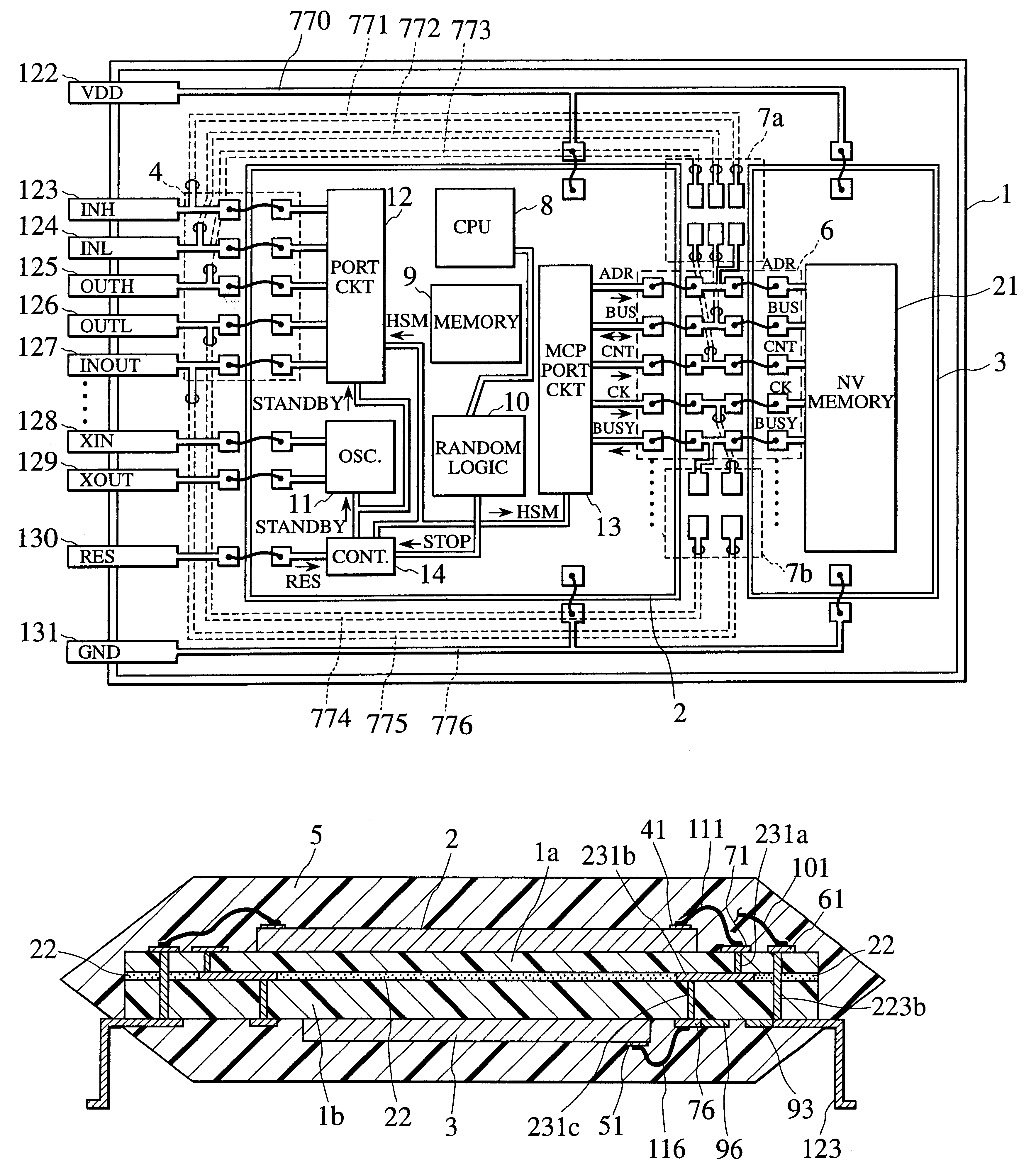
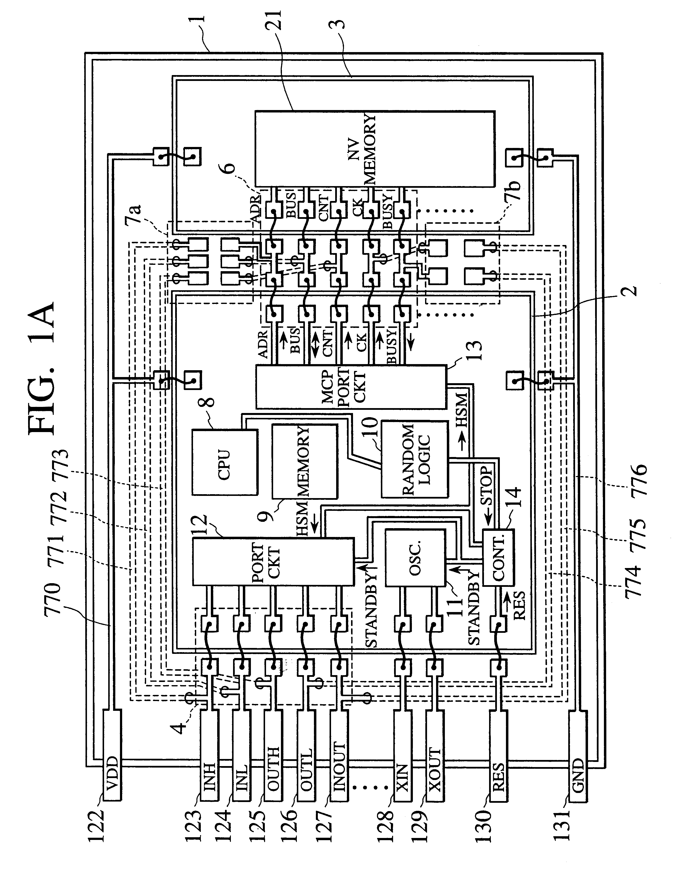
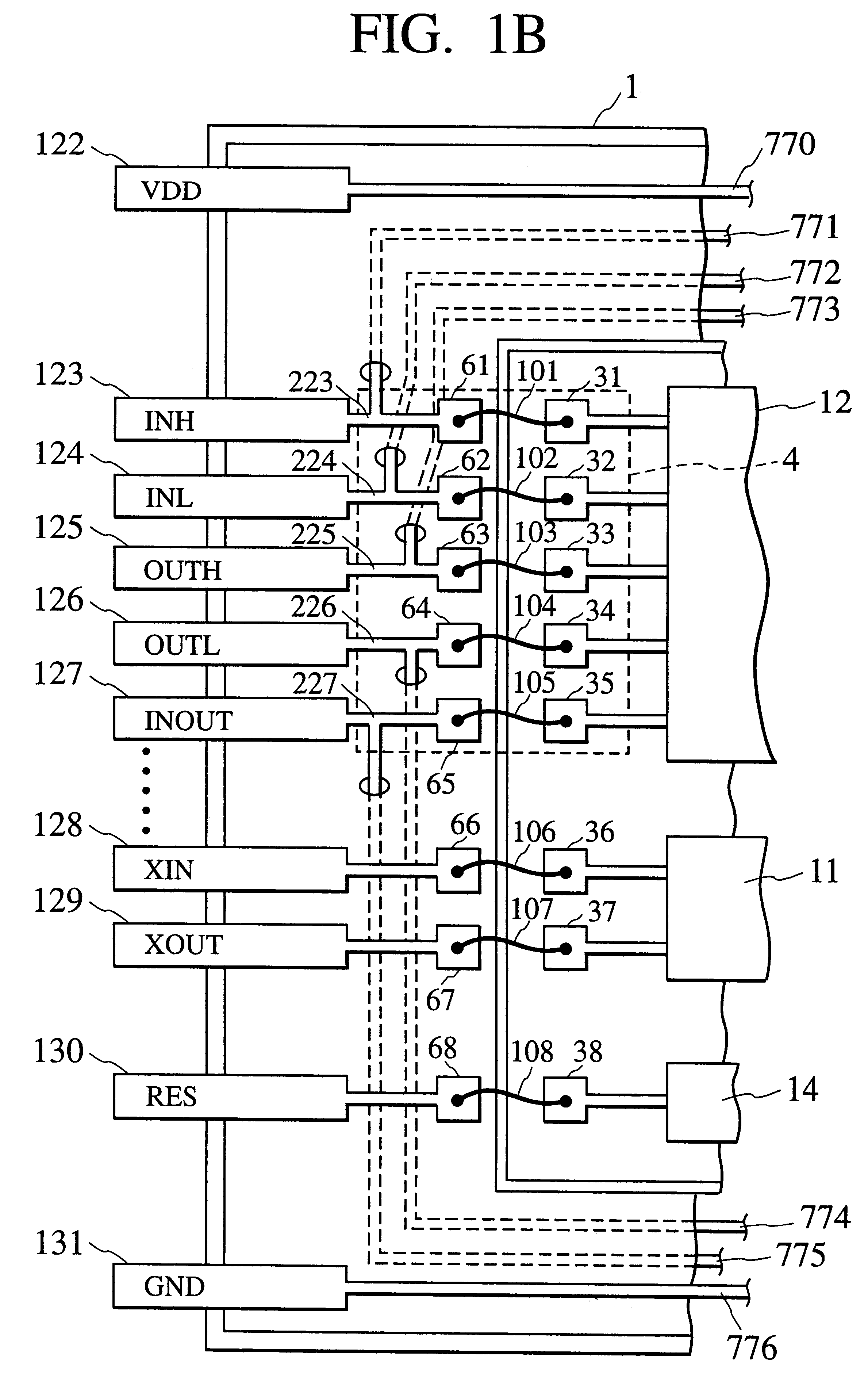
As shown in FIGS. 1A, 1B, and 1C, an MCP according to the present invention has: an MCP substrate 1; a first semiconductor chip 2 and a second semiconductor chip 3 mounted on the MCP substrate 1; MCP leads 123, 124, 125, 127,126 connected to perimeter of the MCP substrate 1; MCP terminal wires 223, 224, . . . , 227 for connecting the MCP leads 123, 124, 125, 127,126 and the first semiconductor chip 2 to each other; interface signal wires 231, 232, . . . , 235 for connecting the first semiconductor chip 2 and the second semiconductor chip 3 to each other; first extra bonding pads 94, 95, . . . , 98 electrically connected to the interface signal wires 231, 232, . . . , 235; and second extra bonding pads 91, 92, 93, 99, and 100 electrically connected to the MCP leads 123, 124, 125, 127,126 and arranged near the first extra bonding pads 94, 95, . . . , 98. The MCP substrate 1 has a laminated multi-layer structure composed of thin-film dielectric and metallization layers, in which buried...

second embodiment

(SECOND EMBODIMENT)

In the above first embodiment, the MCP having a structure in which the CPU chip (first semiconductor chip) 2 and the IP chip (second semiconductor chip) 3 are disposed on a same surface side (the same principal surface side) of the MCP substrate 1 has been explained. In an MCP according to a second embodiment of the present invention, as shown in FIG. 6B, the CPU chip 2 serving as the first semiconductor chip is mounted on the first principal surface (front principal surface) side of a MCP substrate 1, and a IP chip 3 serving as a second chip is mounted on the second principal surface (rear principal surface) side of the MCP substrate 1. Here, "the principal surface" means the surface having the largest area of a slab, or the MCP substrate 1. That is, the second principal surface (rear principal surface) and the first principal surface front principal surface) are major surfaces which are opposing to each other. As shown in FIG. 7A, the CPU chip (first semiconduct...


PUM


Abstract

An MCP has an MCP substrate, first and second semiconductor chips mounted on the MCP substrate, MCP leads connected to perimeter of the MCP substrate. MCP terminal wires disposed on the MCP substrate connect the MCP leads to the first semiconductor chip. Interface signal wires disposed on the MCP substrate connect the first and second semiconductor chips to each other. The MCP further has first and second extra bonding pads. The first extra bonding pad electrically connects to the interface signal wires. The second extra bonding pad electrically connects to the MCP leads. The second extra bonding pad is arranged near the first extra bonding pad. The first and second extra bonding pads are designed to be electrically isolated from each other in a normal usage condition. However, the first and second extra bonding pads are electrically connected to each other when failure analysis is required. Outputs from the port circuit and the MCP port circuit are inhibited by a control circuit mounted on the first semiconductor chip, so that a signal can be exchanged between the second semiconductor chip and an external circuit without using the first semiconductor chip. In this manner, the first and second extra bonding pads are electrically connected to each other, so that the second semiconductor chip can be analyzed, electrically independently of the first semiconductor chip.

Description

1. Field of the InventionThe present invention relates to a multi chip package (MCP) in which first and second semiconductor chips are mounted on a same MCP substrate. In particular, the present invention relates to the MCP in which the second semiconductor chip can be diagnosed independently of the first semiconductor chip, and a method of measuring the electrical characteristics of the second semiconductor chip mounted on the MCP.2. Description of the Related ArtIn recent years, an MCP in which a CPU chip (first semiconductor chip) and an intellectual property (IP) chip (second semiconductor chip) are mounted on an MCP substrate has come to the front. The CPU chip serves as a main and pivotal control chip and configured to perform miscellaneous information processing. And the IP chip exchanges signals with the CPU chip to perform a specific function. In the MCP of this type, the number N.sub.MCP of pins of the MCP is limited by:N.sub.MCP =N.sub.CPU -N.sub.IP (1)Where N.sub.CPU is ...

Claims


Application Information

Patent Timeline
IPC IPC(8): G01R31/28H01L25/065H01L23/495H01L23/48H01L21/822H01L21/66H01L27/04H05K13/08
CPCG01R31/2884H01L23/49531H01L23/49575H01L24/49H01L25/0657H01L24/48H01L2924/014H01L2924/01033H01L2924/20755H01L2924/19107H01L2924/1532H01L2924/01082H01L2924/01079H01L2924/01029H01L2924/01028H01L2924/01013H01L2924/01006H01L2924/01005H01L2924/01004H01L2225/06582H01L2225/06527H01L24/45H01L2224/45015H01L2224/45124H01L2224/45144H01L2224/48091H01L2224/48227H01L2224/4911H01L2224/49171H01L2224/49175H01L2225/0651H01L2924/00014H01L2924/00H01L2924/181H01L2224/05554H01L2924/10162H01L2924/00012H05K13/08
Inventor OIKAWA, KIYOHARU
Owner KK TOSHIBA
Why Eureka
Try Eureka