
Semiconductor device having multilayered gate electrode and impurity regions overlapping therewith

a technology of impurity regions and semiconductor devices, which is applied in the direction of transistors, optics, instruments, etc., can solve the problems of difficult to make an lsi circuit of the tft, line defects, and inability to compare the reliability of the tft utilizing polysilicon to the reliability of the mos

Inactive Publication Date: 2001-07-10
SEMICON ENERGY LAB CO LTD +1
View PDF13 Cites 209 Cited by
  • Summary
  • Abstract
  • Description
  • Claims
  • Application Information

AI Technical Summary

Benefits of technology

The use of the present invention can improve the reliability of an n-channel type TFT used for all kinds of semiconductor devices. As a result, the present invention can improve the reliability of a semiconductor device including a CMOS circuit made of the TFT, to be more specific, the reliability of the pixel matrix circuit of a liquid crystal display device and a driving circuit mounted in the peripheral portion thereof. Additionally, this can improve the reliability of an electronic device in which a semiconductor circuit including the n-channel type TFT and the liquid crystal display device described above are mounted as parts.

Problems solved by technology

In particular, when abnormal conditions occur in a driver circuit, a malfunction occurs in one column (or one row) of the pixel to cause a line defect.
Also, it is said that a TFT utilizing polysilicon is not comparable in reliability to a MOSFET (which is a transistor formed on a single crystal semiconductor substrate) used for an LSI or the like.
There is a growing feeling that it is difficult to make an LSI circuit of the TFT unless this weakness is overcome.
However, the structure disclosed in that paper presents a problem that an off-current (a current flowing when a TFT is in an off-state) increases compared with the conventional LDD structure and hence it was necessary to take countermeasures against the problem.
This TFT structure can fully prevent the deterioration of the on-current, but it has a problem that it has an off-current slightly higher than an ordinary non-overlapped LDD structure.

Method used


Image

  • Semiconductor device having multilayered gate electrode and impurity regions overlapping therewith
  • Semiconductor device having multilayered gate electrode and impurity regions overlapping therewith
  • Semiconductor device having multilayered gate electrode and impurity regions overlapping therewith

Examples


embodiment 1

[Embodiment 1]

The preferred embodiment in accordance with the present invention will be described in detail with reference to FIG. 1 to FIG. 5.

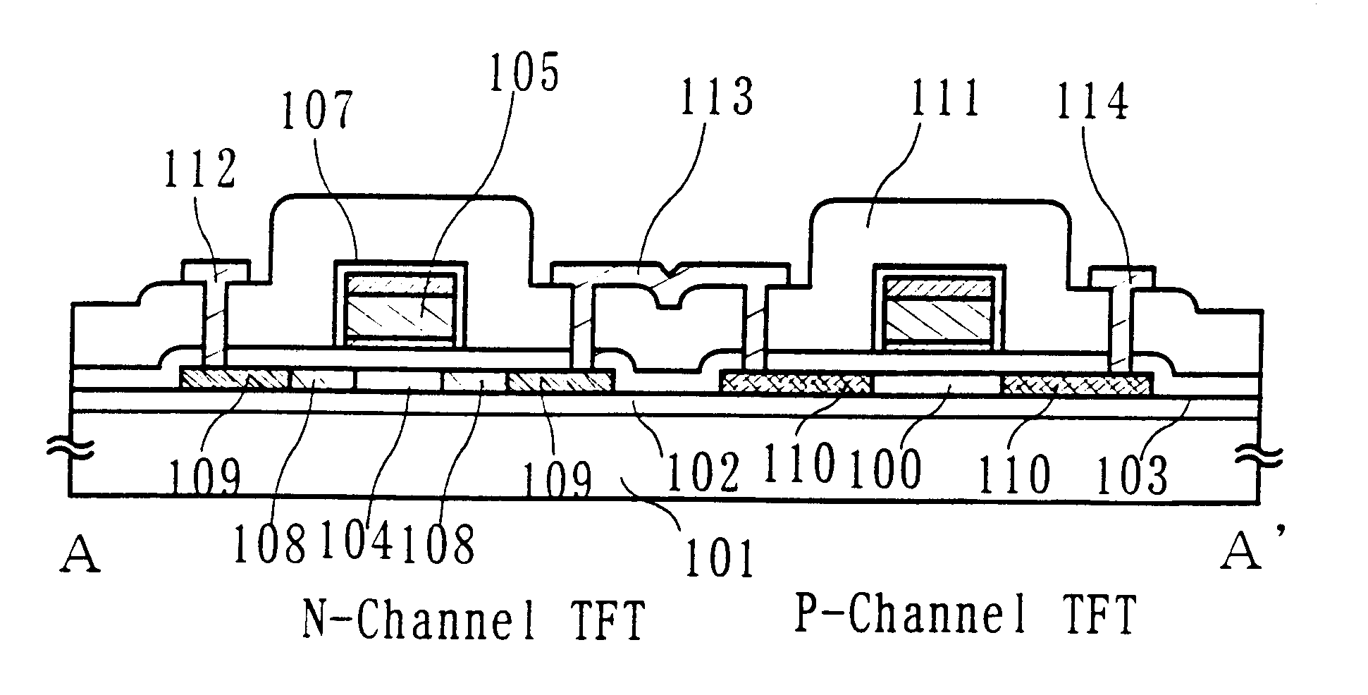
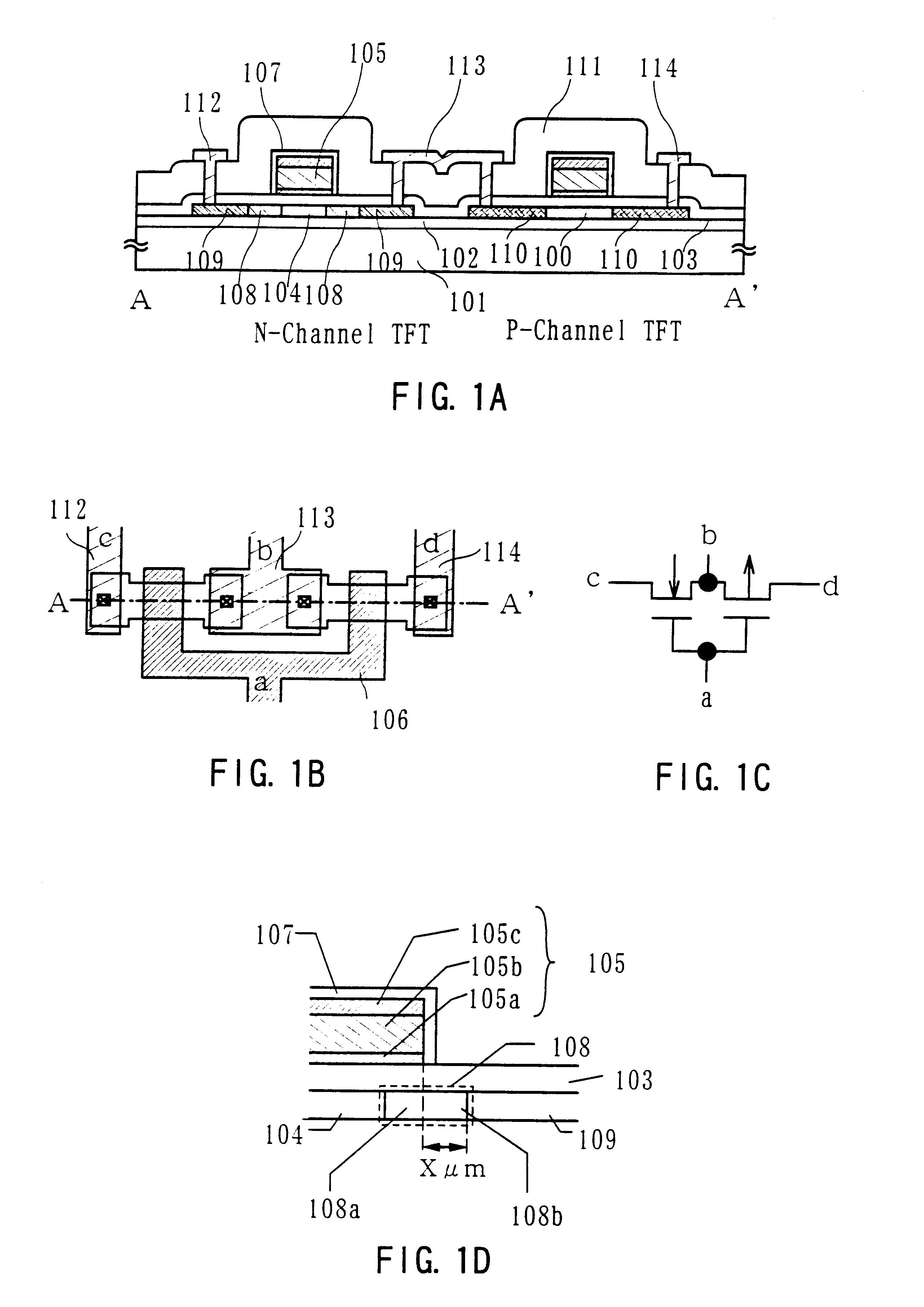
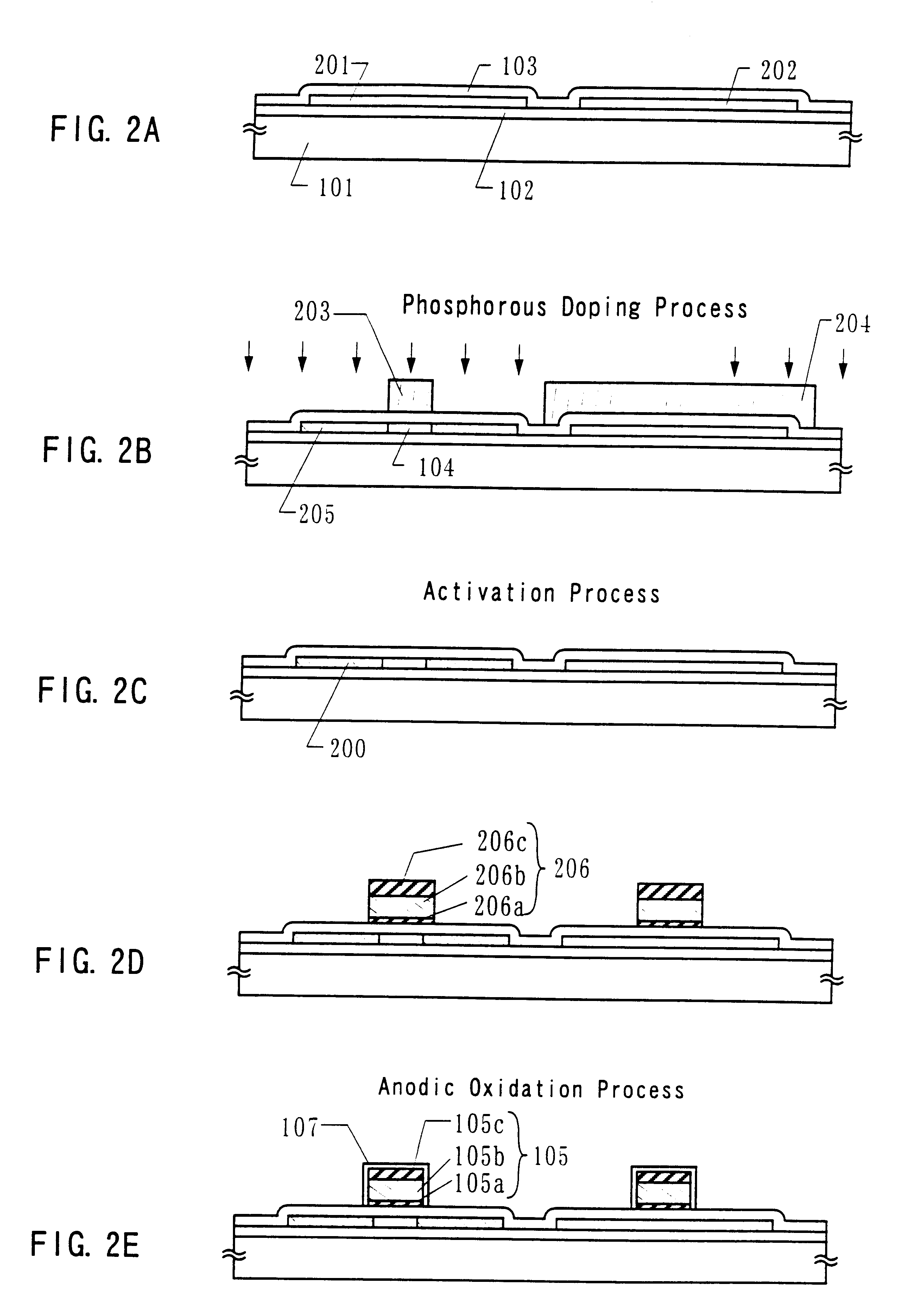
One example of the structure of a semiconductor device provided with a semiconductor circuit including a semiconductor element utilizing the present invention will be described. The semiconductor device in accordance with the present invention has a peripheral driving circuit part and a pixel matrix circuit part on the same substrate. In order to easily show the preferred embodiment, a CMOS circuit constituting a part of the peripheral driving circuit part will be shown in FIG. 1, and a pixel TFT (n-channel type TFT) constituting a part of the pixel matrix circuit part will be shown in FIG. 4.

FIG. 1(B) is an illustration corresponding to the top plan view of FIG. 1(A), and a view taken on chain line A--A ' in FIG. 1(B) corresponds to the cross-sectional structure of the CMOS circuit in FIG. 1(A). Also, FIG. 1(C) is a simplified circuit of the...

embodiment 2

[Embodiment 2]

In the embodiment 2, an example will be described in which a crystalline semiconductor film used as semiconductor layers 201, 202 in the embodiment 1 is formed by a thermal crystallization method using a catalytic element. In the case of using a catalytic element, it is preferable to use technologies disclosed in Japanese Patent Laid-Open No. 7-130652 and Japanese Patent Laid-Open No. 8-78329.

Here, an example will be described in FIG. 6 in which the technology disclosed in Japanese Patent Laid-Open No. 7-130652 is applied to the present invention. First, a silicon oxide film 602 was formed on a substrate 601 and then an amorphous silicon film 603 was formed thereon. Further, a nickel acetate solution containing 10 ppm by weight of nickel was applied thereon to form a nickel-containing layer 604 (see FIG. 6 (A)).

Next, the substrate was subjected to dehydrogenation at 500.degree. C. for one hour and then was subjected to a heat treatment at 550.degree. C. to 650.degree. ...

embodiment 3

[Embodiment 3]

In the embodiment 3, a method in which a crystalline semiconductor film was formed by using an amorphous semiconductor film as a starting film, as is the case with the embodiment 2, and by using the above described catalytic element and then the catalytic element was removed from the crystalline semiconductor film, will be described as a method of forming the semiconductor layers 201, 203 used in the embodiment 1. In the present preferred embodiment 3, the technologies disclosed in Japanese Patent Laid-Open No. 10-135468 or Japanese Patent Laid-Open No. 10-135469 were used as the method.

The technology disclosed in the above references is the one removing a catalytic element used for the crystallization of an amorphous semiconductor film by the gettering action of phosphorus after the crystallization. The concentration of the catalytic element in the crystalline semiconductor film can be reduced to 1.times.10.sup.17 atoms / cm.sup.3 or less, more preferably, 1.times.10.su...


PUM

PropertyMeasurementUnit
thicknessaaaaaaaaaa
thicknessaaaaaaaaaa
lengthaaaaaaaaaa

Abstract

A semiconductor device using a TFT including a multilayered gate electrode and an LDD region partially overlapping with the multilayered gate electrode via a gate insulating film is provided.

Description

1. Field of the InventionThe present invention relates to a method for manufacturing a semiconductor device utilizing a crystalline semiconductor film formed by crystallizing an amorphous semiconductor film, and, in particular, to a semiconductor device of a thin film transistor (hereinafter referred to as a TFT) or the like and a method for manufacturing the semiconductor device. A semiconductor device in accordance with the present invention includes not only a device such as a thin film transistor (TFT), a MOS transistor, or the like, but also a display device having a semiconductor circuit constituted by these insulating gate type transistors and an electrooptical device such as an image sensor, or the like. In addition, the semiconductor device in accordance with the present invention includes an electronic device mounted with the display device and the electrooptical device.2. Description of the Related ArtSince a TFT can be formed on a transparent glass substrate, a developme...

Claims


Application Information

Patent Timeline
Patent Type & Authority Patents(United States)
IPC IPC(8): H01L21/02H01L21/336H01L29/49H01L21/70H01L29/40H01L27/12H01L29/66H01L29/786H01L21/84G02F1/1362G02F1/13H01L21/77
CPCH01L27/1214H01L29/4908H01L29/78621H01L29/78627H01L29/66757G02F1/13454H01L2029/7863H01L27/127
Inventor OHTANI, HISASHIYAMAZAKI, SHUNPEIITOH, MASATAKA
Owner SEMICON ENERGY LAB CO LTD
Features
  • Generate Ideas
  • Intellectual Property
  • Life Sciences
  • Materials
  • Tech Scout
  • Unparalleled Data Quality
  • Higher Quality Content
  • 60% Fewer Hallucinations
Learn More