Thermoelectric module with improved heat-transfer efficiency and method of manufacturing the same

a technology of heat-transfer efficiency and thermoelectric modules, which is applied in the manufacture/treatment of thermoelectric devices, printed circuits, electrical apparatuses, etc., can solve the problems of increasing production costs, reducing the degree of reliability of thermoelectric modules, and low yields of semiconductor-element materials

Inactive Publication Date: 2001-08-14
MATSUSHITA ELECTRIC WORKS LTD
View PDF3 Cites 92 Cited by
  • Summary
  • Abstract
  • Description
  • Claims
  • Application Information

AI Technical Summary

Problems solved by technology

Since these compounds are brittle materials, cracks or chippings of the semiconductor elements easily occur during a manufacturing process of the thermoelectric module, so that there is a problem that the yields of the semiconductor-element materials are low.
This increases the production cost and reduces a degree of reliability of the thermoelectric module.
Since thermal stress occurs according to a difference of thermal expansion coefficient between the semiconductor-element materials and the ceramic-plate material, cracks may be generated in the ceramic plates or the semiconductor elements by the thermal stress.
However, the heat-transfer efficiency of the silicone film 51R is much lower than that of conventional ceramic materials.
Therefore, this thermoelectric module is susceptible to improvement from the viewpoint of heat-transfer efficiency.
In this case, there are problems that the thermal conductivity of the grease material 51S is poor, and the structural stability of the thermoelectric module 1S is low because the heat-transfer plates 52S are merely put on the thermoelectric chip 10S through the grease material 51S.
In addition, when the thickness of the grease material 51S partially becomes small, a short circuit may be caused between the electrodes and the heat-transfer plate.

Method used


Image

  • Thermoelectric module with improved heat-transfer efficiency and method of manufacturing the same
  • Thermoelectric module with improved heat-transfer efficiency and method of manufacturing the same
  • Thermoelectric module with improved heat-transfer efficiency and method of manufacturing the same

Examples


Embodiment Construction

Preferred embodiments of the present invention are explained in detail referring to the attached drawings.

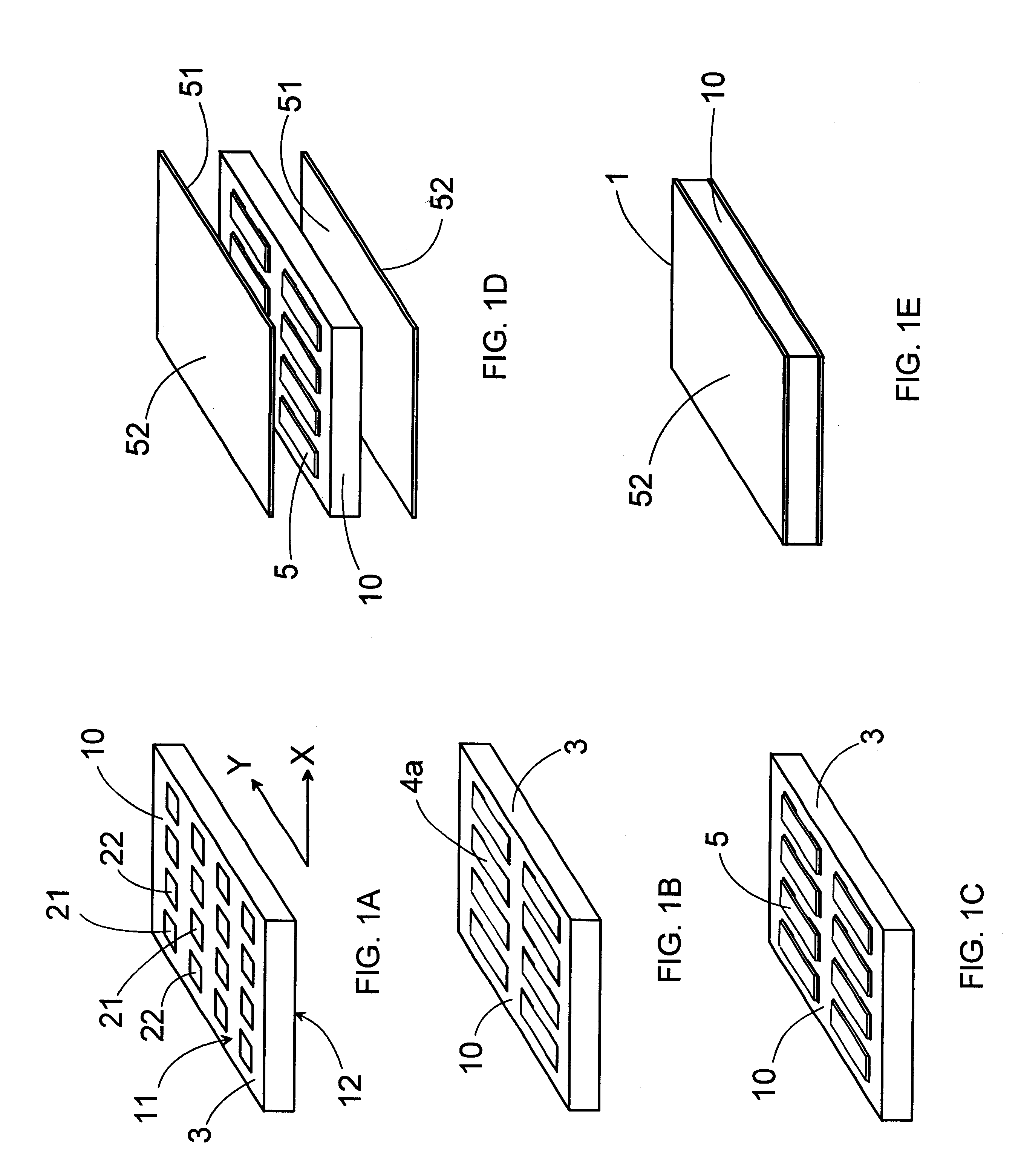
A thermoelectric module of the present invention can be manufactured according to the following method. First, a thermoelectric chip 10 shown in FIG. 1A is prepared. In this embodiment, N-type semiconductor elements 21 made of Bi.sub.2 Te.sub.3 and P-type semiconductor elements 22 made of Sb.sub.2 Te.sub.3 are used as first-type and second-type thermoelectric elements, respectively. The thermoelectric chip 10 has a structure that the N-type and P-type semiconductor elements 21, 22 are arranged in a matrix manner such that each of the N-type semiconductor elements is disposed adjacent to the P-type semiconductor element through a required space in each of X and Y directions, and the space between adjacent semiconductor elements is filled with a first resin 3 having electrical insulation. As the first resin 3, for example, it is possible to use epoxy resins, phenol resins or polyi...


PUM


Abstract

A thermoelectric chip with exposed surfaces of N-type and P-type semiconductor elements on its top and bottom surfaces is prepared by arranging the semiconductor elements in a matrix manner such that each of the N-type semiconductor elements is disposed adjacent to the P-type semiconductor element through a space, and filling the space with a first resin material having electrical insulation. A metal layer is formed on each of the exposed surfaces of the semiconductor elements. Then, first electrodes are formed on the top surface according to a first circuit pattern. Similarly, second electrodes are formed on the bottom surface according to a second circuit pattern different from the first circuit pattern. An electrical insulation sheet of a second resin material containing a ceramic powder with high thermal conductivity is bonded to the top and bottom surfaces to obtain the thermoelectric module.

Description

1. Field of the InventionThe present invention relates to a thermoelectric module that is a temperature control device using Peltier effect, and particularly a thermoelectric module with improved heat-transfer efficiency, and a method of manufacturing the thermoelectric module.2. Disclosure of the Prior ArtAs shown in FIGS. 10A and 10B, a conventional thermoelectric module 1P has a structure comprising an arrangement of N-type semiconductor elements 21P and P-type semiconductor elements 22P, which are arranged in a matrix manner such that each of the N-type semiconductor elements 21P is disposed adjacent to the P-type semiconductor element 22P through a required space, upper electrodes 5P disposed on a top surface of the arrangement to connect between adjacent semiconductor elements 21P and 22P according to a first circuit pattern, lower electrodes 6P disposed on a bottom surface of the arrangement to connect between adjacent semiconductor elements 21P and 22P according to a second ...

Claims


Application Information

Patent Timeline
Patent Type & Authority Patents(United States)
IPC IPC(8): H01L35/32H01L35/34H01L35/00H05K1/00H01L35/28
CPCH01L35/34H01L35/32H10N10/01H10N10/17H10N10/81H10N10/851H10N10/856H10N10/13
Inventor YOSHIOKA, HIROKAZUKAMADA, KAZUOURANO, YOJIKOBAYASHI, KENTARO
Owner MATSUSHITA ELECTRIC WORKS LTD
Why Eureka
Try Eureka