Method for buried plate formation in deep trench capacitors

a capacitor and trench capacitor technology, applied in the direction of basic electric elements, electrical equipment, semiconductor devices, etc., can solve the problems of difficult formation of buried plates, and achieve the effect of simplifying the manufacturing process flow

Inactive Publication Date: 2001-08-28
IBM CORP
View PDF7 Cites 39 Cited by
  • Summary
  • Abstract
  • Description
  • Claims
  • Application Information

AI Technical Summary

Benefits of technology

The method of the present invention offers significant advantages in terms of final test yields, cost reduction, reproducibility, reliability, uniformity and manufacturing process flow simplification.

Problems solved by technology

Difficulties have been experienced in forming the buried plate in the deep trenches.

Method used


Image

  • Method for buried plate formation in deep trench capacitors
  • Method for buried plate formation in deep trench capacitors
  • Method for buried plate formation in deep trench capacitors

Examples


Embodiment Construction

The buried plate formation process specifically includes the eight basic steps recited below.

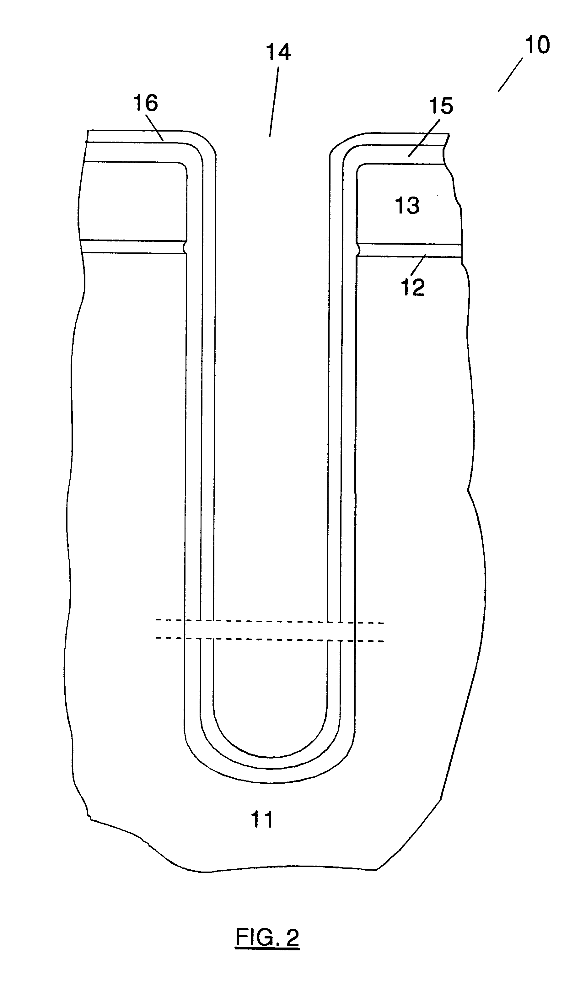
(1) Depositing a conformal layer of arsenic-doped silicon glass (ASG) onto the structure.

(2) Depositing a conformal layer of SiO.sub.2 atop said ASG layer.

(3) Filling the deep trenches with a photoresist layer.

(4) Removing the photoresist material down to a given depth into deep trenches.

(5) Removing SiO.sub.2 and ASG materials from unprotected areas.

(6) Stripping remaining photoresist layer from the bottom of deep trenches.

(7) Out-diffusing arsenic from the ASG layer into the silicon substrate.

(8) Finally, removing SiO.sub.2 and ASG materials from the bottom of deep trenches.

All these processing steps are conducted in the Deep Trench Module.

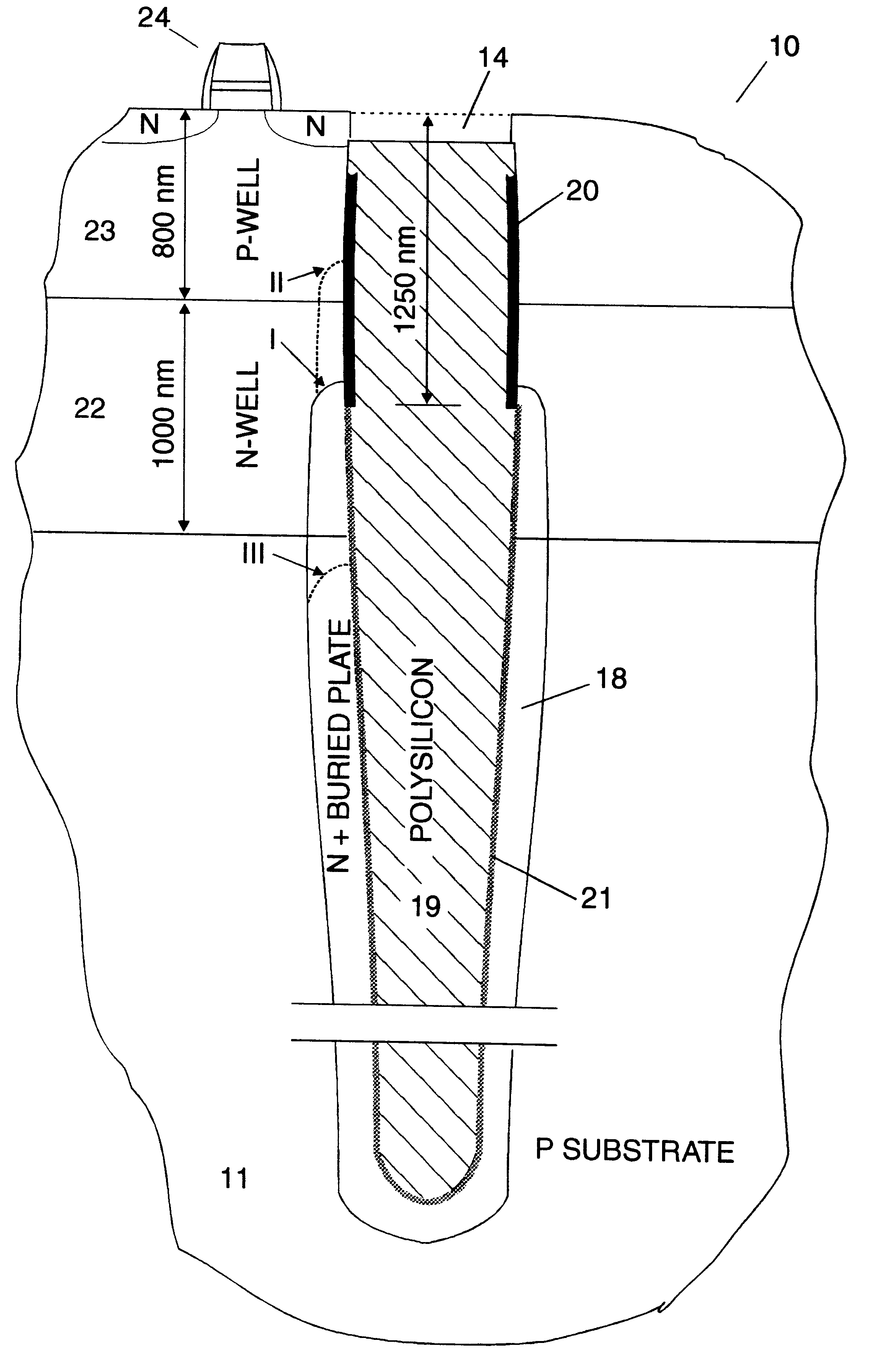
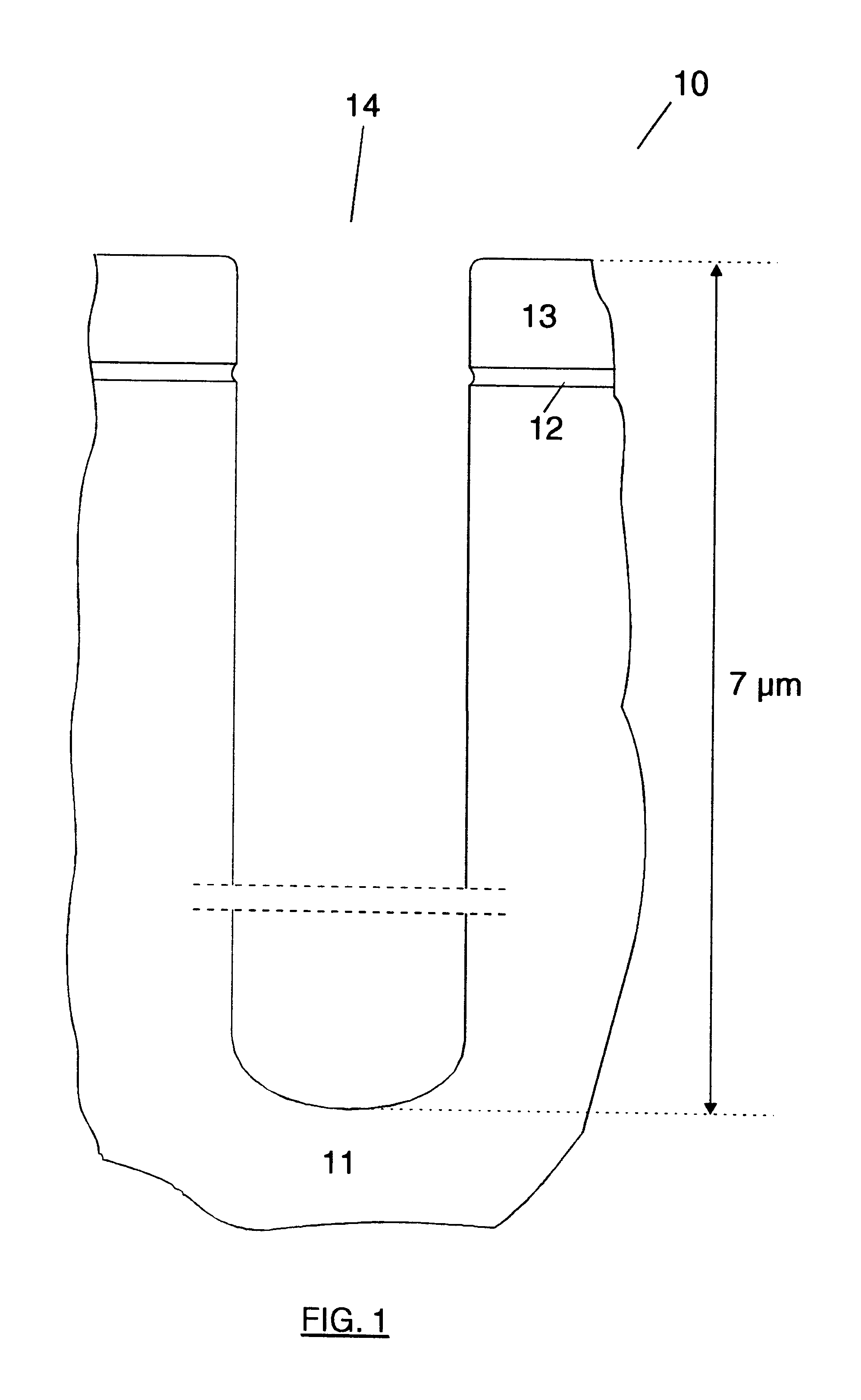
FIG. 1 schematically illustrates the starting structure mentioned above bearing numeral 10 consisting of a P-type silicon substrate 11 with a 10 nm thick silicon oxide (SiO.sub.2) and a 220 nm thick silicon nitride (Si.sub.3 N.sub.4) layers respectively ...


PUM


Abstract

An improved method of forming the buried plate regions in deep trench capacitors used in DRAM memory semiconductor circuits in which the polymer used in the deep trench is etched down to the desired depth in a reactive ion etch tool using an O2/CF4 chemistry. Since optical/interferometric etch end-point detection system can be used to monitor the etch back step in its totality, the quantity of the polymer remaining in deep trenches can be very accurately controlled, which in turn will produce a well controlled buried plate region during the out-diffusion step of the arsenic dopant contained in the arsenic doped silicon glass layer.

Description

The present invention relates to the manufacture of semiconductor integrated circuits (Ics) and more particularly to an improved method for forming the buried plate regions in deep trench capacitors of DRAM memory chips.Deep trenches are extensively used in the manufacture of semiconductor integrated circuits, in particular of 64 and 256 Mb DRAM memory chips to define the storage capacitors. Basically, a deep trench is formed in a doped silicon substrate, then a dielectric film is conformally deposited thereon to coat the entire interior surface of the trench and finally the trench is filled with doped polysilicon. This doped silicon / dielectric film / doped polysilicon forms the storage capacitor. In order to keep an acceptable capacitor value in spite of continuous capacitor size reduction, the thickness of the capacitor dielectric film is constantly reduced. In turn, the voltage across dielectric film must be drastically reduced to avoid undesired breakdown voltage effects. In order...

Claims


Application Information

Patent Timeline
Patent Type & Authority Patents(United States)
IPC IPC(8): H01L21/70H01L21/02H01L21/311H01L21/8242
CPCH01L27/1087H01L21/31138H10B12/0387
Inventor CORONEL, PHILIPPECRUAU, DAVIDLEVERD, FRANCOISMACCAGNAN, RENZOMASS, ERIC
Owner IBM CORP
Why Eureka
Try Eureka