Digital delay line with low insertion delay

a delay line and low insertion delay technology, applied in the field of digital circuits, can solve the problems of delay elements consuming significant chip space, longer propagation times, and inability to carry out intended functions

Inactive Publication Date: 2001-09-04
IBM CORP
View PDF11 Cites 30 Cited by
  • Summary
  • Abstract
  • Description
  • Claims
  • Application Information

AI Technical Summary

Problems solved by technology

However, some signal paths will necessarily have longer propagation times than others, and intended functions cannot be carried out unless proper signals are simultaneously present.
However, it should be appreciated that delay elements can consume significant amounts of chip space, depending on the maximum amount of delay to be accommodated or provided.
However, the mere inclusion of a DLL provides some delay time that cannot be avoided.
This clock cycle jump increases the vulnerability of the computer system to operational errors caused by occasional variations in the output of an associated power...

Method used


Image

  • Digital delay line with low insertion delay
  • Digital delay line with low insertion delay
  • Digital delay line with low insertion delay

Examples


Embodiment Construction

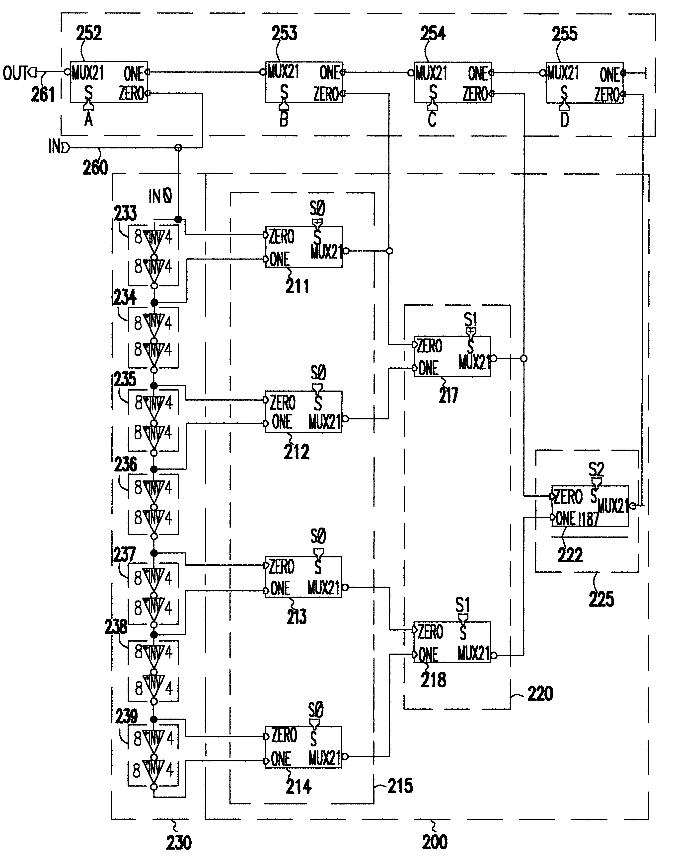
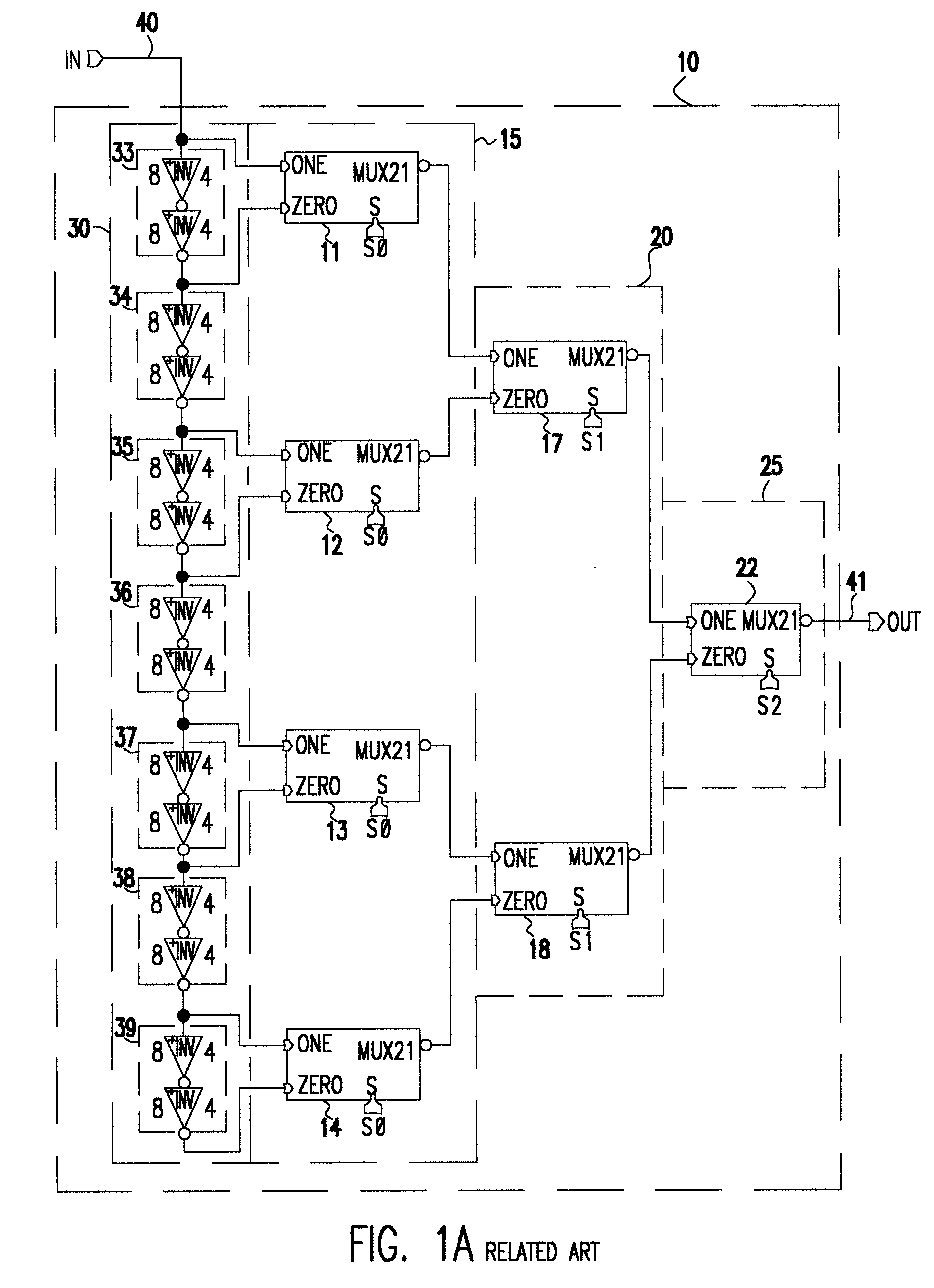
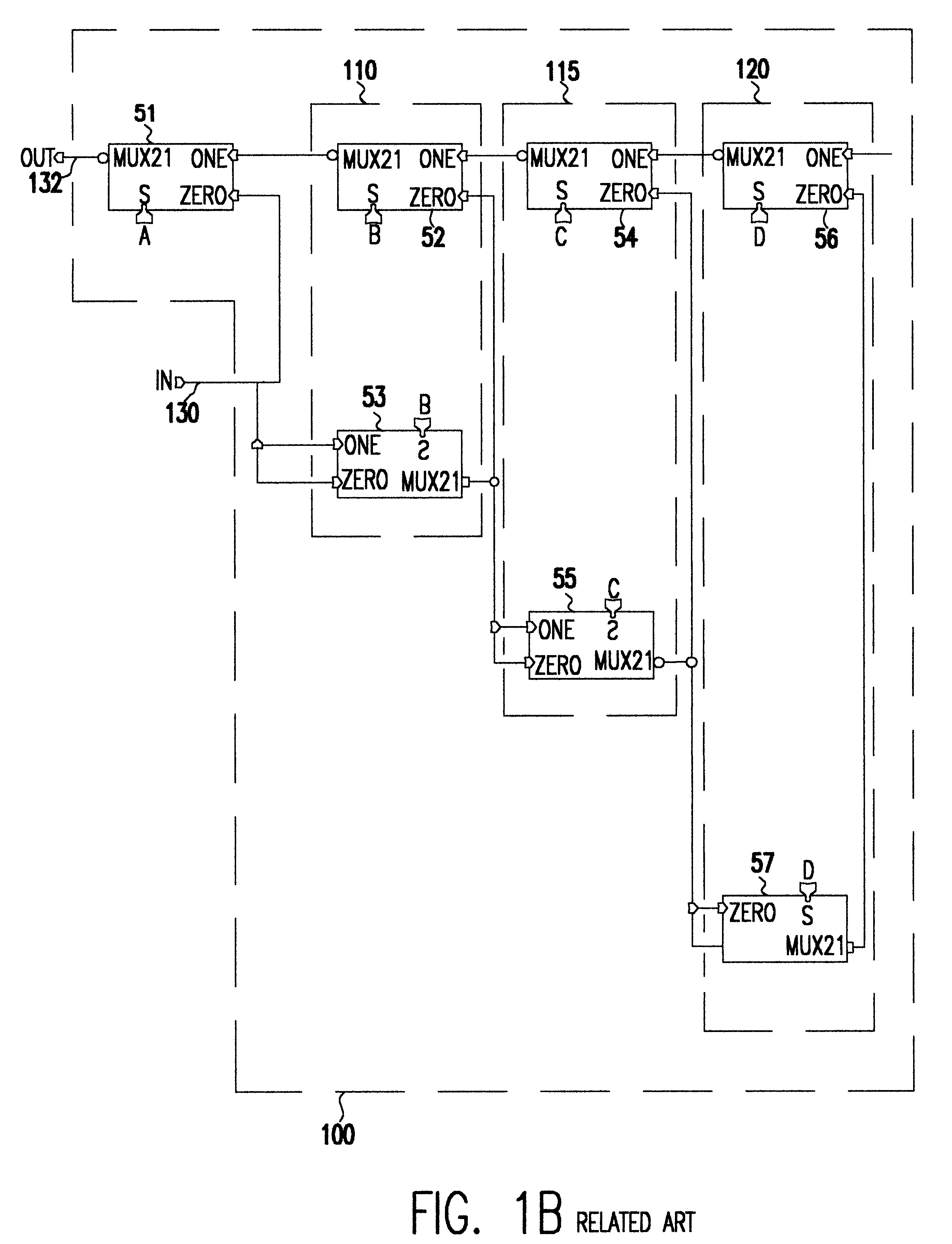
Referring now to the drawings, and more particularly to FIG. 1A, there is shown a schematic diagram of a first alternative embodiment of a delay line over which the present invention is an improvement. It is not admitted that the delay line shown in FIG. 1A is prior art. FIG. 1A is provided to facilitate an understanding of the present invention. Accordingly, FIG. 1A is labeled as "Related Art".

In this embodiment, a multiplexer (mux) array 10 contains seven 2:1 muxes wherein the outputs of four muxes 11-14 in a first logic layer 15 become the inputs to two muxes 17-18 in a second logic layer 20, and the outputs of the muxes 17-18 in the second logic layer 20 become the inputs to the seventh mux 22 which alone constitutes a third logic layer 25. The propagation delay through the three layers illustrated 15, 20, and 25 is equal to three times the delay through a single 2:1 mux. More logic levels could, of course, be provided for a larger delay range (or higher delay resolution or a co...


PUM


Abstract

A variable digital delay line with an insertion delay as low as a single delay element yet capable of providing a large programmable delay with a small simple control mechanism. A loop connects an input to an output through selectable first delay elements such as 2:1 muxes and selectable second delay elements such as pairs of inverters by way of a plurality of intermediate nodes having a tap. A plurality of sneak paths are available wherein the loop by passes a remainder of first delay elements and/or second delay elements by way of the taps at the intermediate nodes.

Description

DESCRIPTION1. Field of the InventionThe present invention generally relates to digital circuits for providing a delay of digital signals, and more particularly to programmable delay lines for correction, synchronization, and minimization of propagation times of digital signals.2. Description of the Prior ArtModern digital logic circuits such as digital logic circuits that are included in digital data processors are characterized by short signal propagation times which are enhanced by decreased switching element (e.g. transistor) sizes and increased integration density. The short signal propagation times are exploited by reducing clock cycle times so that logic functions and data processing can be carried out more rapidly. However, some signal paths will necessarily have longer propagation times than others, and intended functions cannot be carried out unless proper signals are simultaneously present. This synchronization becomes more critical as clock cycle times are reduced.It is a...

Claims


Application Information

Patent Timeline
IPC IPC(8): H03K5/13H03K5/00
CPCH03K5/131H03K5/133H03K2005/00058
Inventor CHU, ALBERT M.FERRAIOLO, FRANK D.FIFIELD, JOHN A.NGUYEN, TERESA THISOFRANKO, MICHAEL
Owner IBM CORP
Why Eureka
Try Eureka