Low-voltage differential-signalling output buffer with pre-emphasis

a low-voltage differential and output buffer technology, applied in pulse manipulation, pulse technique, baseband system details, etc., can solve the problems of long time-consuming and laborious driving of low-impedance transmission lines, distortion, and large external loads that cannot be quickly driven with such wide voltage swings without creating emi and distortions

Inactive Publication Date: 2001-09-11
DIODES INC
View PDF17 Cites 81 Cited by
  • Summary
  • Abstract
  • Description
  • Claims
  • Application Information

AI Technical Summary

Problems solved by technology

While such TTL or full-level signals are useful to provide wide noise margins, large external loads cannot quickly be driven with such wide voltage swings without creating electro-magnetic interference (EMI) and distortions.
Driving low impedance transmission lines has long been a problem.
Distortions can occur, further reducing the opening of the eye pattern due to jitter and noise of the cable environment.
This limits operation at higher frequencies.

Method used


Image

  • Low-voltage differential-signalling output buffer with pre-emphasis
  • Low-voltage differential-signalling output buffer with pre-emphasis
  • Low-voltage differential-signalling output buffer with pre-emphasis

Examples


Embodiment Construction

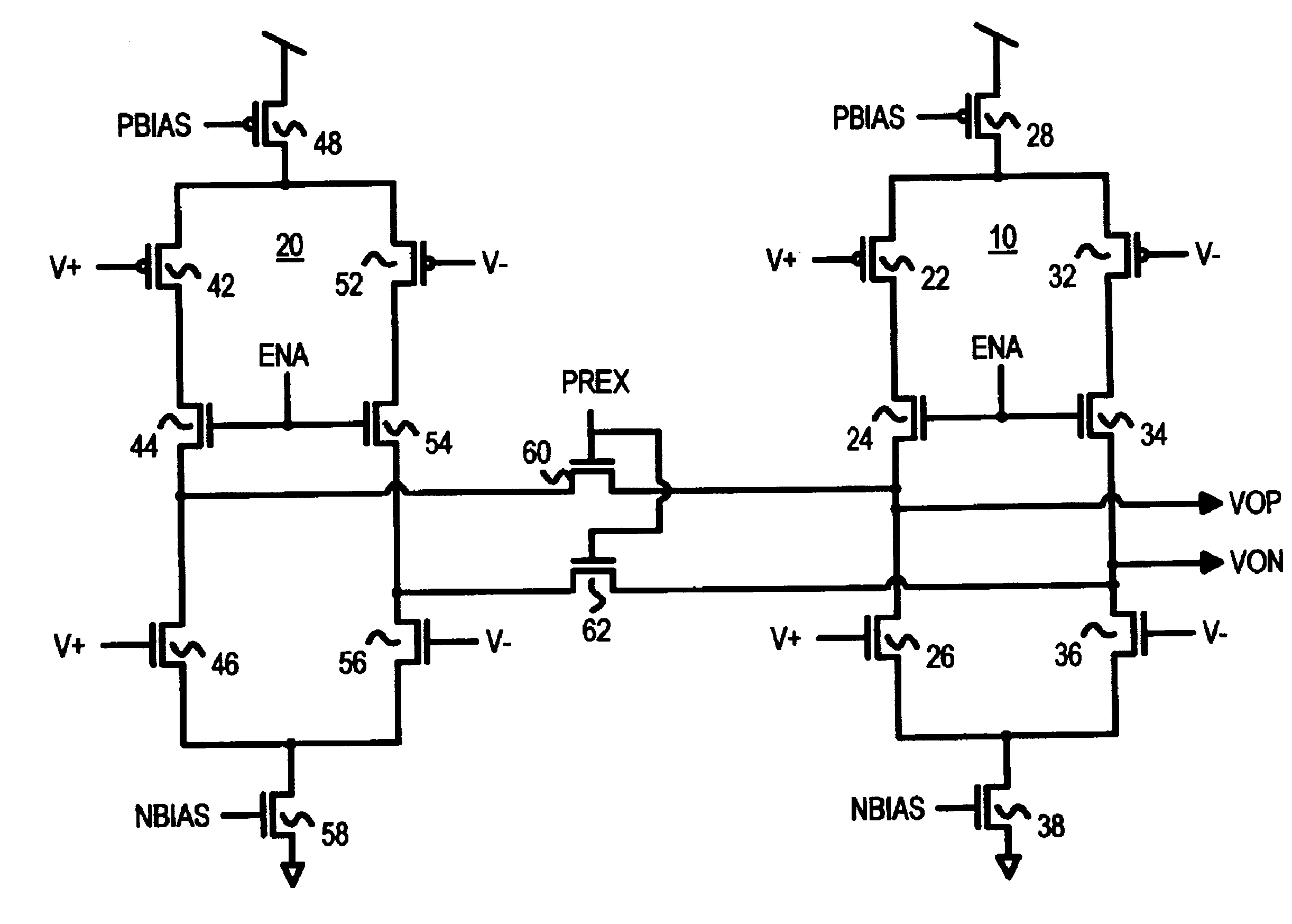
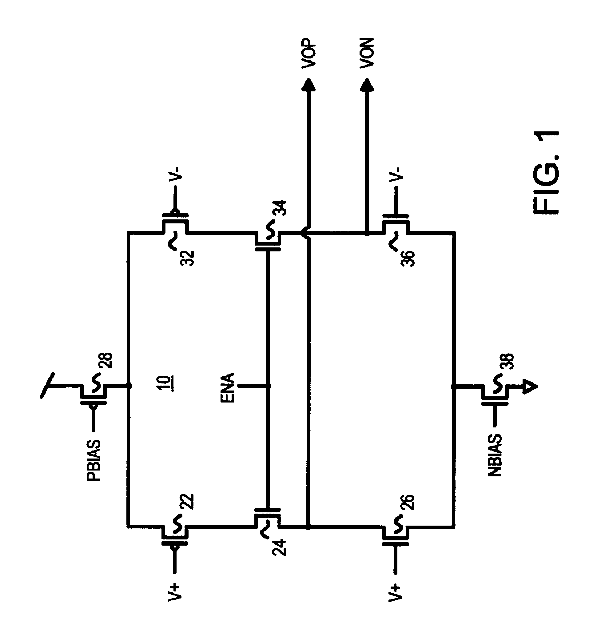
Several other embodiments are contemplated by the inventor. For example, full transmission gates can be substituted for the n-channel link transistors. Different transistor sizes and biases can be used to obtain desired currents in the two stages. The load resistance may be chosen by the system designer from a range of values. Additional devices such as capacitors can be added, and various parasitic resistances and capacitances may exist but are not shown. The pulse generator can be constructed in many variations, such as using NAND gates and signal inversion rather than NOR gates as shown. Positive logic gates may be used, such as an OR gate constructed from a NOR gate and an inverter as is commonly available from standard-cell libraries. More complex multi-input gates can also be employed.

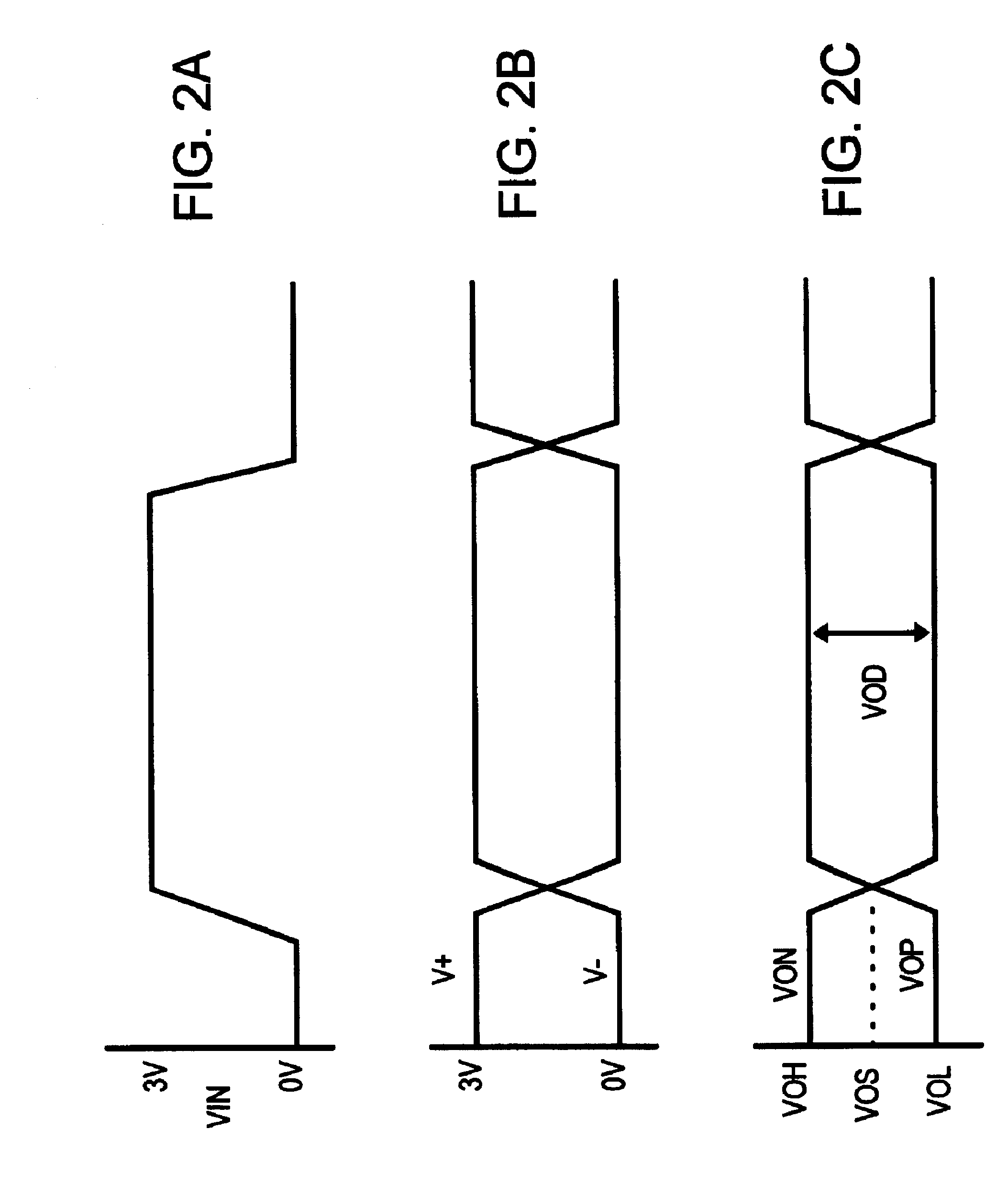
Additional boost or primary stages may be included. Separate timing signals may be used to provide a gradual increase or decrease in switching currents. The voltage differences (VOD) shown are ac...


PUM


Abstract

A low-voltage differential signaling (LVDS) output buffer has an improved eye pattern. The LVDS buffer has two parallel stages. A primary stage generates enough current to generate a first voltage drop across a load resistor. At higher frequencies, parasitic capacitive coupling reduces this first voltage drop, closing the eye pattern. A boost stage generates an additional boost current through the load resistor, adding to the voltage drop and opening the eye pattern. The boost stage is coupled to the outputs by link transistors that are enabled by a pre-emphasis signal generated by resetable pulse generators. When outputs switch, the pre-emphasis signal pulses the link transistors on, adding the boost current. At high frequencies, the pulse generators are reset before the pre-emphasis signal ends. The boost current is continuously added at high frequencies, but at low frequencies the boost current only occurs during the pre-emphasis period after outputs switch.

Description

BACKGROUND OF INVENTIONThis invention relates to CMOS output buffers, and more particularly to low-voltage differential-signaling output buffers.A variety of electronic systems rely on improvements in high-speed signaling to increase performance. Networks can operate at higher data rates when signals are propagated more quickly between stations and within network switches. Computers process data at a higher rate when the data can be sent to memory and peripherals at higher speeds. Telephone systems can handle more calls when faster transmission occurs.One of the bottlenecks to improved performance is external signaling, when signals are driven from an integrated circuit (IC) to another IC. Metal traces on a printed-circuit board (PCB) must be driven by the IC's output buffer. These metal traces are much larger than the metal lines on the IC itself and thus have a higher capacitive and resistive load. Some signals need to be drive off the PCB across cabling, perhaps to other rooms or...

Claims


Application Information

Patent Timeline
Patent Type & Authority Patents(United States)
IPC IPC(8): H03K5/22H04L25/02H03K5/24
CPCH03K5/2481H04L25/0272H04L25/0292H04L25/028
Inventor WONG, ANTHONY YAP
Owner DIODES INC
Why Eureka
Try Eureka