Optical device

a technology of optical devices and optical bonding, which is applied in the direction of optical waveguide light guides, optical elements, instruments, etc., can solve the problems of reducing the efficiency of the device, reducing the horizontal mode quality, and unable to achieve the bonding efficiency of the single-mode waveguid

Inactive Publication Date: 2001-09-11
NEC CORP
View PDF10 Cites 30 Cited by
  • Summary
  • Abstract
  • Description
  • Claims
  • Application Information

AI Technical Summary

Problems solved by technology

However, in case that such a multi-mode semiconductor laser is used as an excitation light source for the waveguide laser / amplifier, an optical bonding to the single-mode waveguide cannot be achieved at a higher efficiency due to the lower horizontal mode quality.
Accordingly, a problem arises that a lower efficiency of a device (light / light conversion efficiency) is likely to occur.

Method used


Image

  • Optical device
  • Optical device
  • Optical device

Examples


first embodiment

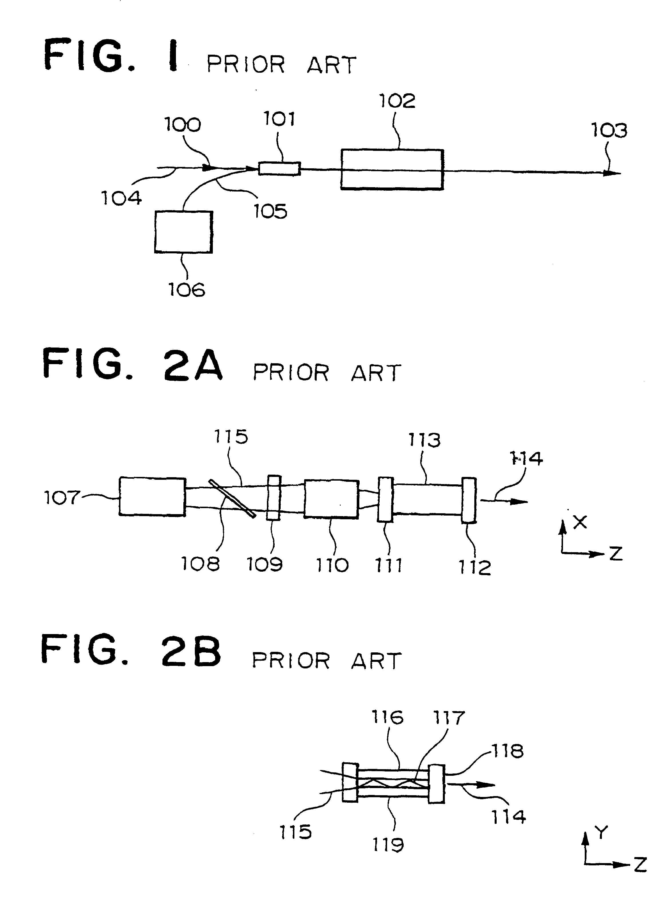
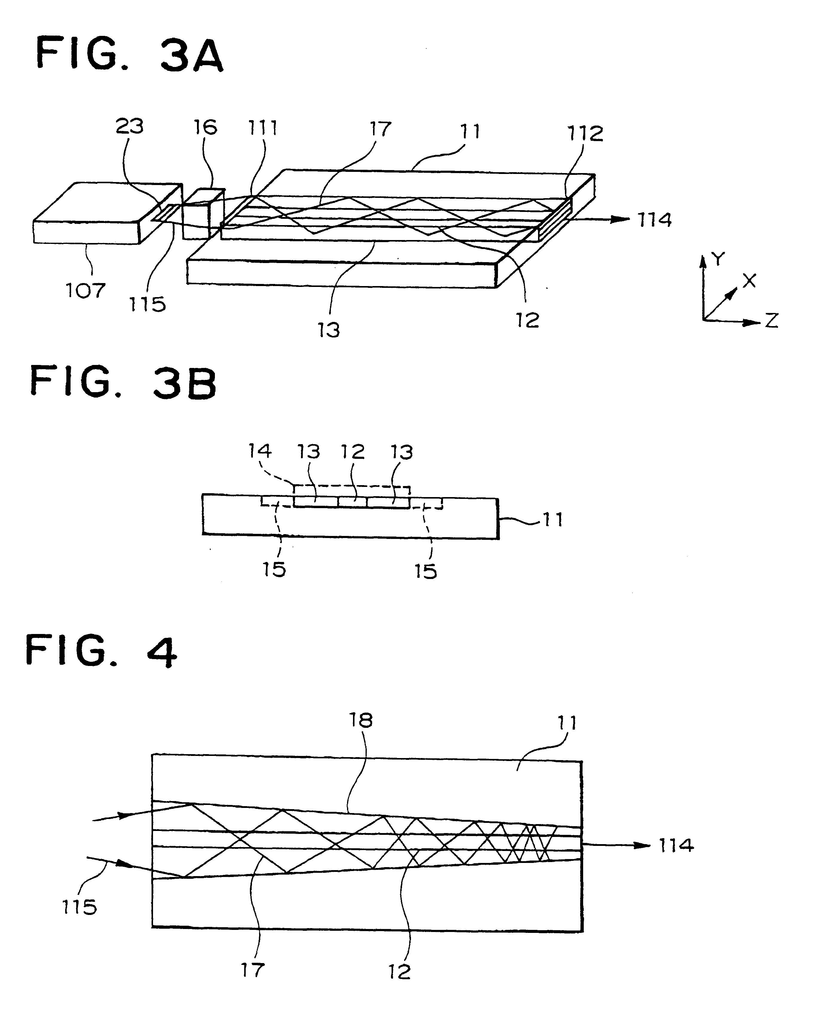
Now, the present invention is more specifically described with reference to accompanying drawings in which description of similar elements to those of FIGS. 1, 2A and 2B is omitted by affixing the same numerals thereto.

A waveguide lasing apparatus shown in FIG. 3A includes a multi-mode semiconductor laser 107, an excitation optical system 16 and an external resonator. A width of an active layer (light generation layer) 23 is between 20 .mu.m and 500 .mu.m, desirably between 50 .mu.m and 200 .mu.m. This is because the width of the semiconductor laser light generating width is desirably narrower for bonding with a single-mode waveguide 12 and a width of the single-mode waveguide 12 of the external resonator is generally between 6 and 10 .mu.m, and some extent of the light generation width is required for the higher output.

The optical waveguide used in the external resonator includes the single-mode waveguide 12 and multi-mode waveguides 13 on an optical substrate (for example, made of...

second embodiment

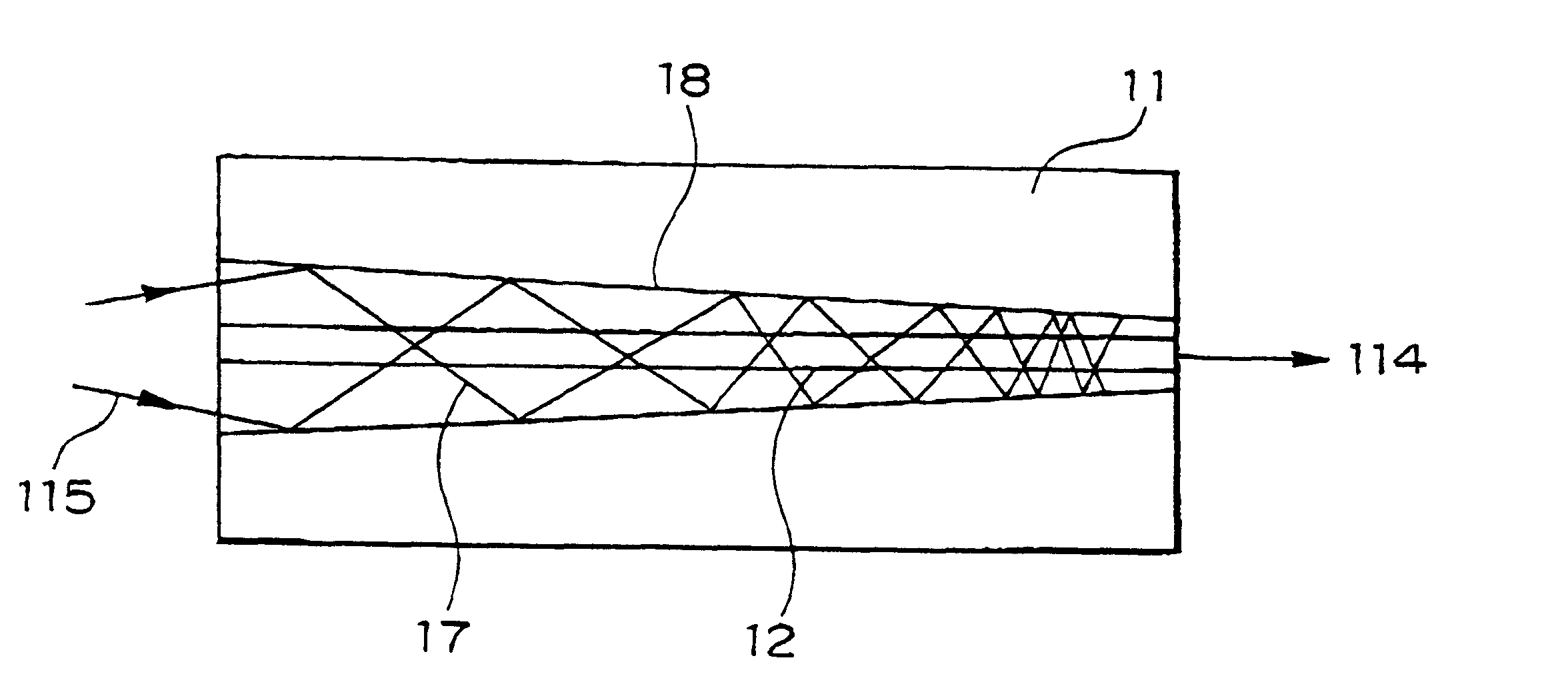
In the present invention, a waveguide structure is not restricted to that of the first embodiment, and various structures of effectively absorbing an exciting ray can be employed.

As a second embodiment, a preferred example thereof will be described.

Referring to FIG. 4, a waveguide of the present embodiment different from that of the first embodiment shown in FIGS. 3A and 3B includes a tapered multi-mode waveguide 18 of which a width is reduced towards a propagation direction of an exciting ray. Since the propagating exciting ray 17 is confined in a narrower space in such a tapered structure, the absorption rate of the exciting ray in the propagation step can be made larger than that when the width of the waveguide is fixed. For example, when the width of the waveguide at the incident facet was 30 .mu.m and that at the output facet was about 15 .mu.m, an absorption rate was obtained at a waveguide length of 5.7 mm while a waveguide length of 7.5 mm was needed for obtaining a similar ...

third embodiment

A third embodiment exemplifies a waveguide laser having a higher output than that of the first embodiment

The waveguide laser of the present embodiment shown in FIG. 5 is different from that shown in FIGS. 3A and 3B in that a waveguide of an input side of a multi-mode waveguide 13 includes a plurality of multi-mode waveguides 21. Also in the respective multi-mode waveguides 21, an exciting ray propagates in a single-mode in a thickness direction and in a multi-mode in a width direction. These multi-mode waveguides 21 are combined to form a single waveguide by means of a wave adder 20.

The respective multi-mode semiconductor lasers 19 (excitation optical systems are not shown) are mounted on input facets of the multi-mode waveguides 21. In place of the multi-mode semiconductor lasers 19, a so-called "semiconductor laser bar" including light generating elements disposed in an array having a space among them three or four times larger than a light generation width can be used.

Similarly t...


PUM


Abstract

An optical waveguide including a single-mode waveguide in which an induced radiation ray generated by exciting the ion propagates in a single-mode in both of a thickness direction and a width direction in the single-mode waveguide; and multi-mode waveguides disposed along both of side surfaces of the single-mode waveguide in which the ray propagates in a single-mode in a thickness direction of the multi-mode waveguide and propagates in a multi-mode in a width direction. In accordance with the present invention, the exciting ray is easily absorbed because the ray propagates to cross the single-mode waveguide without a skew-mode propagation, and the laser and the photo-amplifier which can obtain a higher output in the single-mode is provided.

Description

(a) Field of the InventionThe present invention relates to an optical device which is used for implementing an external resonator lasing with a solid laser or an optical amplifier, and a laser and a laser amplifier employing an optical waveguide.(b) Description of the Related ArtAn optically excited laser / amplification device has been recently researched which contains a rare-earth element (Er.sup.3+, Nd.sup.3+, Yb.sup.3+, Tm.sup.3+, Ho.sup.3+ and Pr.sup.3+) or a transition metal (Ti, Cr) as active species and glass or crystals as a host material. A typical example includes a solid laser excited by a semiconductor laser and an Er.sup.3+ doped fiber amplifier excited by a semiconductor laser. As a further advanced form, a compact and rigid active device is known which is formed by integrating a waveguide type laser and a waveguide type laser amplifier on a single silicon substrate or a quartz substrate to realize functions such as light modulation and switching on the single substrat...

Claims


Application Information

Patent Timeline
Patent Type & Authority Patents(United States)
IPC IPC(8): H01S3/06H01S3/063H01S3/0941G02B6/12G02B6/122H01S3/10
CPCH01S3/063H01S3/0632H01S3/2308H01S3/094084H01S3/09415H01S3/094057
Inventor KASAMATSU, TADASHI
Owner NEC CORP
Why Eureka
Try Eureka