Method for improving wiring related yield and capacitance properties of integrated circuits by maze-routing

Inactive Publication Date: 2001-10-16
IBM CORP
View PDF3 Cites 44 Cited by
  • Summary
  • Abstract
  • Description
  • Claims
  • Application Information

AI Technical Summary

Benefits of technology

1) Reduced likelihood of random shorts, which in turn improves circuit yield. The yield is modeled using the average critical area measure, which is equal to the summation of L/S, where L is the common run length between two adjacent wires of the routing, and S is the spacing between the adjacent wires. The smaller the average critical area results in a better IC yield.
2) Reduced wiring capacitance which improves circuit performance and reduces power consumption. The wiring capacitance can be estimated by the formula A.times.W.times.L+B.times.L/S.sup.K, where A, B and K are constants that depend on technology parameters and

Problems solved by technology

Channel routing techniques are mostly interesting as a research tool but are seldom used in practice, mainly because of the aforementioned wiring versus area tradeoff.
This approach suffers from certain fundamental limitations, such as the applicabil

Method used


Image

  • Method for improving wiring related yield and capacitance properties of integrated circuits by maze-routing
  • Method for improving wiring related yield and capacitance properties of integrated circuits by maze-routing
  • Method for improving wiring related yield and capacitance properties of integrated circuits by maze-routing

Examples


Example

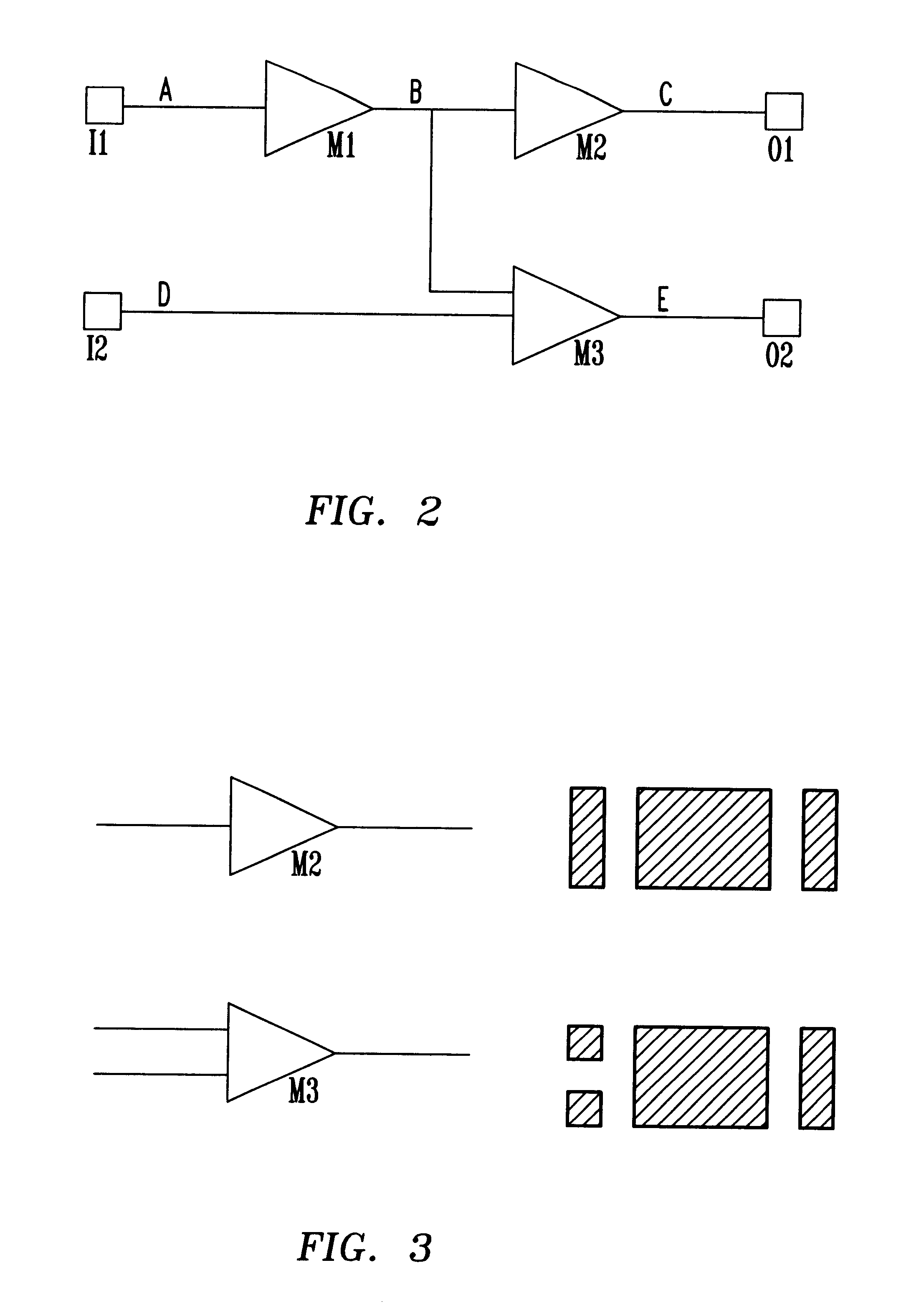
Referring now to FIG. 2, there is shown a schematic diagram of an IC consisting of cells M1, M2, and M3, two inputs I1 and I2, and three outputs O1, O2 and O3. The circuit consists of net A connecting I1 to M1; net B connecting M1, M2 and M3; net C connecting M2 to O1; net D connecting I2 to M3, and net E connecting M3 to O2. The circuit shown is a logic (or electrical) representation of the illustrative circuit used to describe how the cells are placed and routed.

FIG. 3 shows each cell of the logic configuration converted to a physical design. The shapes depicted are required to manufacture the IC chip. They represent the locations of the pins of each cell which tell the router which of the shapes need to be connected. The physical cells are placed on the IC chip during the placement phase and subsequently wired.

FIG. 4 illustrates the placement of the cells forming the IC chip of FIG. 1. The nets are referenced by I1, I2, M1, M2, M3, O1 and O2. Nets A, B, C, D, and E are shown insi...


PUM


Abstract

A method for automatically wiring (i.e., routing) an integrated circuit chip after completing the placement of cells on the chip is described. The method employs a maze routing such that the spacing between the routed wires is increased, while at the same time maintaining control over the total wiring length. The maze routing herein described is modified to improve chip yield, reduce wiring capacitance, limit power consumption and coupled signal noise, all of which are achieved by increasing wire-to-wire spacings.

Description

This invention generally relates to VLSI circuit design, and more specifically to a method for performing automatic wiring of an integrated circuit chip, module or card.Automatic routing of VLSI chips, modules or cards can be accomplished by a variety of methods, many of which have been known and studied for at least 20 years. It is acknowledged by practitioners that automatic routing consists of two stages: a Global Routing, which produces rough locations of wires, and a Detailed Routing, which takes the results of the global routing to generate detailed locations and layers for wiring the chip.Automatic routing has been enhanced by taking into consideration certain relevant factors which improve the electrical characteristics of the package being wired. Some of these techniques have been described in the literature, examples of which are listed below:S. Y. Kuo, "YOR: an yield optimizing routing algorithm by minimizing critical areas and vias," published in the IEEE Transactions on...

Claims


Application Information

Patent Timeline
IPC IPC(8): G06F17/50
CPCG06F17/5077G06F30/394
Inventor TELLEZ, GUSTAVODOYLE, GARYHONSINGER, PHILIPLOVEJOY, STEVENMEILEY, CHARLESSTARKEY, GORDENWILCOX, JR., REGINALD
Owner IBM CORP
Why Eureka
Try Eureka