Method for manufacturing bonded wafer and bonded wafer

a technology of bonded wafers and manufacturing methods, applied in the direction of instruments, natural mineral layered products, transportation and packaging, etc., can solve the problems of inferior bonding, long time-consuming and labor-intensive thin film making, and waste of material application

Inactive Publication Date: 2001-11-06
SHIN-ETSU HANDOTAI CO LTD
View PDF9 Cites 74 Cited by
  • Summary
  • Abstract
  • Description
  • Claims
  • Application Information

AI Technical Summary

Benefits of technology

In another aspect of the present invention, if carbon concentration at a joint surface after separation heat treatment is 3.times.10.sup.14 atoms / cm.sup.2 or less, it is possible to prevent a void from being generated by its subsequent bonding heat treatment.
Preferably, a thickness of a silicon oxide film present at close contacted surfaces is 0.1 .mu.m or more, thereby the occurrence of void caused by the bonding heat treatment can be positively prevented.
In a further aspect of the present invention, if the surfaces of wafers to be bonded from each other are cleaned with ozone cleaning and / or sulfuric acid-hydrogen peroxide cleaning combined with at least one of SC-1 cleaning and SC-2 cleaning, thereafter the wafers are bonded to each other, carbon concentration at the close contacted and joint surfaces can be positively reduced to such a level that no void is generated.
As described above, the present invention can suppress inferior bondings in which after performing the separation heat treatment, delamination does not occur at the ion implanted layer, but either an entire surface or its part is separated at the close contacted portions, and although a void (partial unbonded portion) is not generated after performing a separation heat treatment, but void is generated after performing a bonding heat treatment, when the bonded wafer is manufactured by hydrogen ion delamination method. Accordingly, the bonded wafer having no separation state or void at the bonding interface can be provided in a superior productivity and under a low cost.

Problems solved by technology

However, it was made thin through grinding and polishing, resulting in that it took much time for making a thin film, useless application of material was set and uniformity of film thickness of only about .+-.0.3 .mu.m of a target film thickness was attained.
However, the present inventors found that the following two kinds of inferior bonding occurred frequently while the bonded wafer was being made in repetition by the hydrogen ion separation method.

Method used


Image

  • Method for manufacturing bonded wafer and bonded wafer
  • Method for manufacturing bonded wafer and bonded wafer

Examples


embodiment

Preferred Embodiment

Example 1

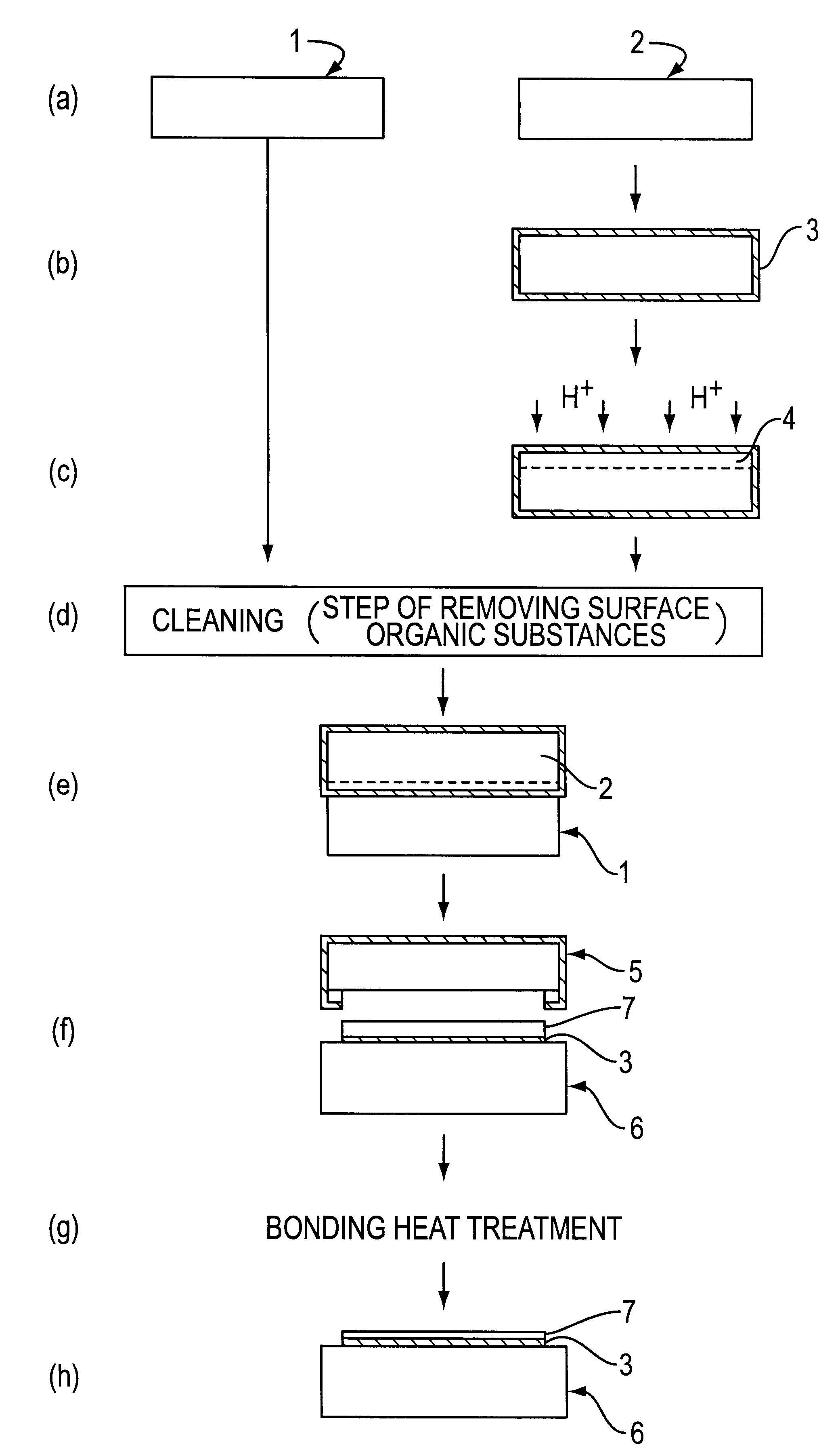
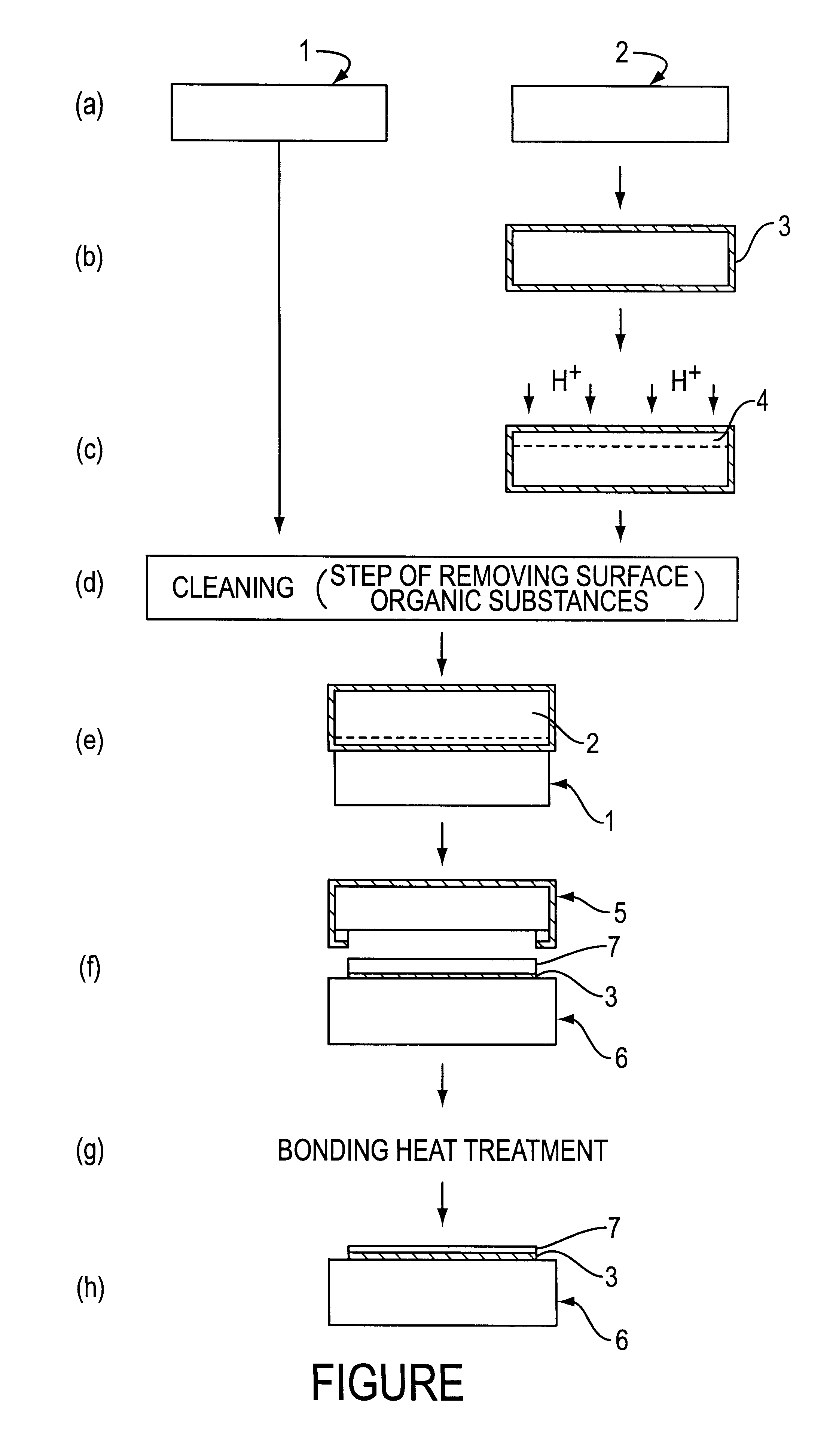
At first, two single-crystal silicon wafers 2 having a diameter of 150 nm, a thickness of 625 .mu.m, a conductive p-type, and a resistivity of 10 to 20 .OMEGA..multidot.cm with its one surface being polished in mirror surface were prepared, one of the wafers was formed as a bond wafer and an oxide film having a thickness of 0.1 .mu.m was formed at the surface by a thermal oxidation.

Then, H+ions were implanted at the mirror surface side of the bond wafer through an oxide film under a condition of an implanting energy of 40 keV and an implanting dose 8.times.10.sup.14 atoms / cm.sup.2, thereafter sulfuric acid-hydrogen peroxide cleaning (96% concentrated sulfuric acid:30% H.sub.2 O.sub.2 =6 kg:100 cc, a liquid temperature of 110.degree. C.) was carried out for 5 minutes, rinsed with pure water, thereafter SC-1 cleaning (29% NH4OH aqueous solution:30% H.sub.2 O.sub.2, pure water=1: 1: 8, a liquid temperature of 80.degree. C.) was carried out for 4 minutes, an...

example 2

The bond wafer in which the wafer of the same kind as that of the preferred embodiment 1 was not formed with an oxide film, but ion implanted under the same condition was manufactured and kept in a desiccator containing dibutylbenzoquinone therein for 1 hour.

After this period, the cleaning with sulfuric acid-hydrogen peroxide was not carried out, but only the SC-1, SC-2 and SC-1 cleanings were carried out under the same condition as that of the preferred embodiment 1 together with the base wafer and after drying them, both wafers were closely contacted to each other at a room temperature, the same separation heat treatment and bonding heat treatment as those of the preferred embodiment 1 were carried out in sequence. As a result, several voids with a diameter of about 2 to 10 mm were generated at the SOI wafer after the separation heat treatment and their numbers at the SOI wafer were increased after the bonding heat treatment was carried out. However, a phenomenon in which the enti...

example 3

Except the fact that an oxide film with a thickness of 0.1 .mu.m was formed at the bond wafer, a plurality of SOI wafers were manufactured in which operations up to the bonding heat treatment were carried out in sequence under the same condition as that of the preferred embodiment 2. As a result, no voids were observed at all at any kinds of SOI wafers after performing the separation heat treatment, although there occurred cases in which several voids were generated after performing the bonding heat treatment and the other cases in which voids were not generated at all.


PUM

PropertyMeasurementUnit
thicknessaaaaaaaaaa
temperatureaaaaaaaaaa

Abstract

The object of the invention is to provide a bonded wafer in which an inferior bonding state of the bonded wafer attained by a hydrogen ion delamination method is reduced, no separation or no void is found at the connecting interface under a superior production characteristic and in a low cost. In a method for manufacturing a bonded wafer by a hydrogen ion delamination method, carbon concentration at a close contacted surface where both wafers are closely contacted from each other is 3-1014 atoms / cm2 or less.

Description

1. Field of the InventionThis invention relates to a method for reducing an inferior bonding at a joint surface in a so-called hydrogen ion delamination (separation) method (also called as a smart-cut method) in which joined SOI wafers, at least one wafer being ion implanted, are heat treated to cause separation to SOI wafers and delaminated wafers, thereafter the SOI wafers are heat treated to make bonding firmly.2. Description of the Related ArtAs a method of manufacturing an SOI (silicon on insulator) wafer under application of a bonding method, it has been well known in the related art to provide a technology for bonding two silicon wafers through a silicon oxide film, for example, a method for forming an oxide film on at least one wafer, closely contacting these wafers to each other without placing any foreign materials at the joint surface, thereafter heat treating them at a temperature of about 200 to 1200.degree. C. to increase a bonding strength, as disclosed in the gazette...

Claims


Application Information

Patent Timeline
Patent Type & Authority Patents(United States)
IPC IPC(8): H01L21/762H01L21/02H01L21/70H01L21/20H01L21/306H01L21/265H01L27/12
CPCH01L21/02052H01L21/2007H01L21/76254Y10T428/265Y10S438/974H01L21/265
Inventor YOKOKAWA, ISAOMITANI, KIYOSHI
Owner SHIN-ETSU HANDOTAI CO LTD
Why Eureka
Try Eureka