Semiconductor device and fabrication process thereof

a semiconductor and semiconductor technology, applied in the direction of semiconductor devices, electrical devices, transistors, etc., can solve the problems of leakage current, power consumption also increases, leakage current does not decline sufficiently,

Inactive Publication Date: 2002-01-08
DENSO CORP
View PDF26 Cites 22 Cited by
  • Summary
  • Abstract
  • Description
  • Claims
  • Application Information

AI Technical Summary

Problems solved by technology

However, in an enhancement-type ROM structure, as described above it is difficult to withstand voltage in a region of the channel region contiguous to the drain region 15a when compared when; ion implantation is not performed (i.e., when a high-concentration P-type region is not formed), this results in a problem in which leakage current from the drain region 15a to the substrate 11 or source region 15b is generated.
Power consumption also increases.
However, it was understood that even when a high-concentration P-type region is not formed on the drain region side, if an end portion of the high-concentration P-type region is proximate to an end portion of the drain region, leakage current does not decline sufficiently.
Consequently, it becomes still more difficult for the depletion layer extending toward the high-concentration region to reach the high-concentration region.
That is to say, it becomes more difficult for the depletion layer to reach the high-concentration region at a time of rated-voltage application.

Method used


Image

  • Semiconductor device and fabrication process thereof
  • Semiconductor device and fabrication process thereof
  • Semiconductor device and fabrication process thereof

Examples


first embodiment

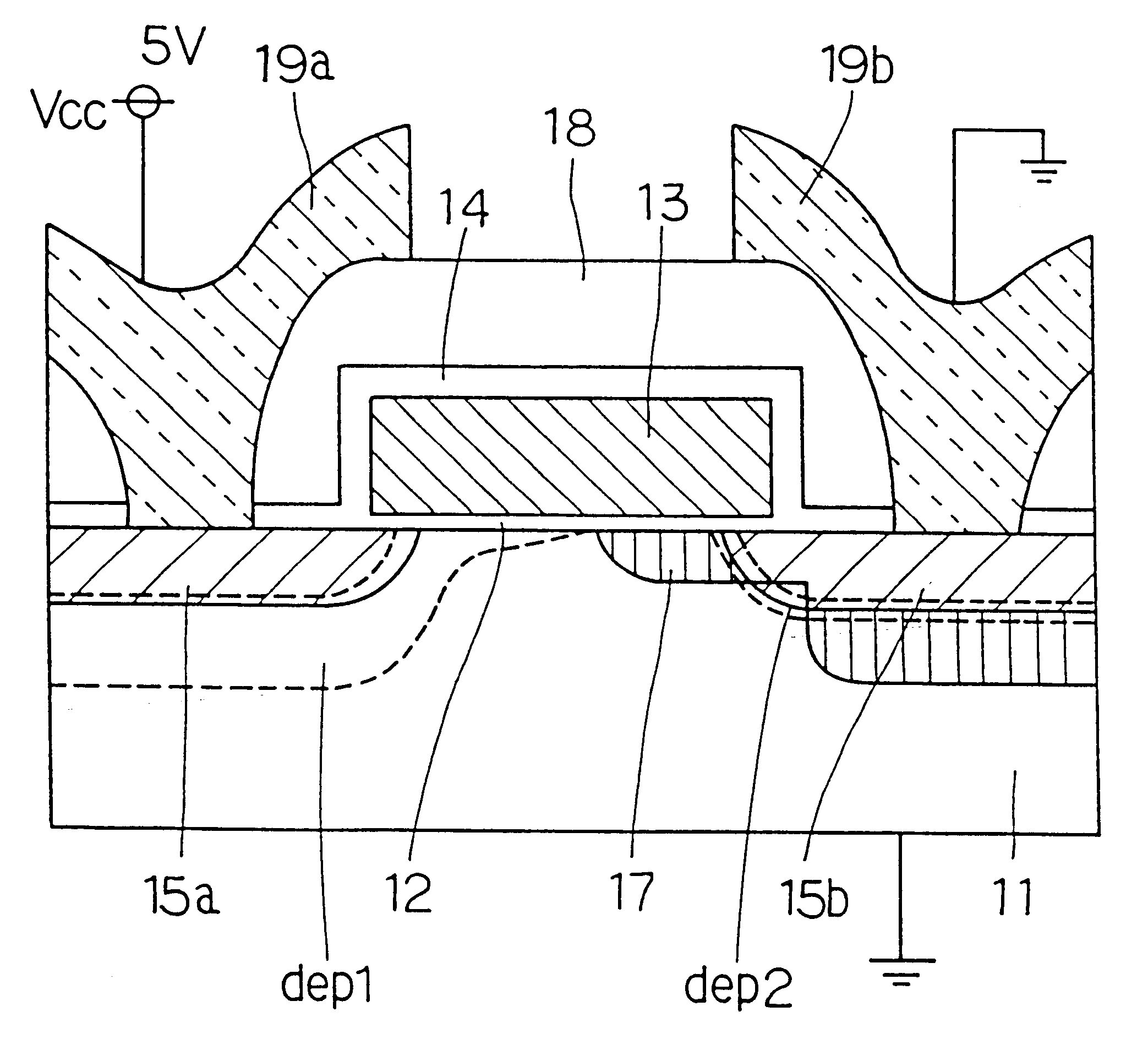
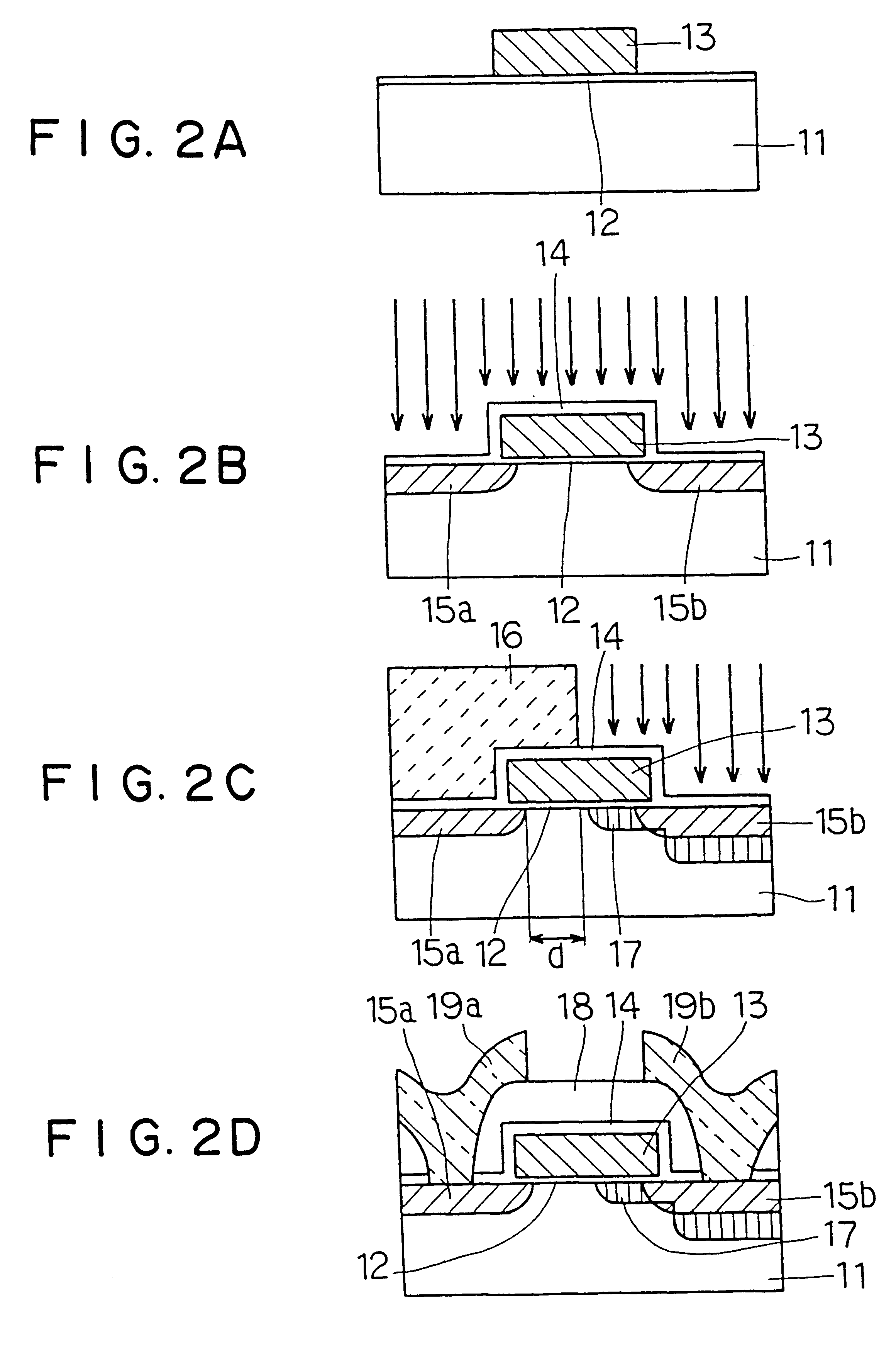
FIG. 1 shows the present invention, and indicates a sectional view of a ROM as a semiconductor memory device which is one enhancement-type transistor.

In a MOS transistor having a gate oxide film 12 on a P-type semiconductor substrate (or P-type well region provided in a substrate) 11 and a polycrystalline silicon gate electrode 13 provided further thereabove, a high-concentration P-type region 17 formed by implantation acceptor dopant (for example boron) is formed only in a proximity of a source region 15b, and is structured so that the high-concentration P-type region 17 is not contiguous with a drain region 15a.

In FIG. 1, dotted lines in the proximity of the source and drain regions show expansion states of depletion layers extending under a condition that a drain voltage is set at 5V while a gate voltage, a source voltage and substrate voltage are set at 0V. The depletion layer (dep2) on the side of the source region 15b extends a small amount, but the depletion layer (dep1) on t...

second embodiment

FIG. 9 indicates a second embodiment according to the present invention.

In this second embodiment, both a drain region 15a and a source region 15b are set such that a high-concentration P-type region 17 is not contiguous. FIG. 9 indicates a portion corresponding to the step in FIG. 2C.

In an enhancement-type ROM obtained by the step indicated in this FIG. 9, heavily leakage current is not generated even when high potential with respect to a substrate 11 is applied to both the drain region 15a and the source region 15b. Moreover, because the source and drain regions can be utilized oppositely, there exists an advantage that a degree of freedom in circuit design is improved.

third embodiment

FIG. 10 indicates a third embodiment according to the present invention.

In this third embodiment, in contrast to the above-described first embodiment, ion implantation to cause threshold voltage to be raised is performed from an oblique direction (approximately 45 degrees is employed as an implantation angle .theta.) to form a high-concentration P-type region 17. FIG. 10 indicates a portion corresponding to the step in FIG. 2C.

In this case, when acceleration voltage (or cceleration energy) at a time of ion implantation is regulated, i.e., established so that ions injected from a side surface 131 of a gate electrode 13 reach a channel region and ions injected from an upper surface 132 of the gate electrode 13 do not reach the channel region, ions reach only a proximity of the source region 15b, and an effect similar to the first embodiment is obtained.

A concept of a method of regulation of acceleration voltage in ion implantation will be described with reference to FIGS. 11A through ...


PUM


Abstract

A semiconductor device having an enhancement-type MOS structure which can prevent large leakage current is disclosed. A high-concentration region for threshold-value regulation use formed in a channel region below a gate electrode in an enhancement-type transistor is caused to be contiguous with a source region and not contiguous with a drain region. Herein, the distance between the high-concentration region and the drain region is set so as to preclude the depletion layer extending from the drain region side from reaching the high-concentration region. Therefore, the electrical field in the depletion layer does not become the critical field which causes avalanche or Zener breakdown, and so leakage current can be caused to be reduced.

Description

This application is based upon and claims the benefit of priority of the prior Japanese Patent application No. 6-289883 filed on Nov. 24, 1994, the contents of which are incorporated herein by reference.1. Field of the InventionThe present invention relates to an enhancement-type semiconductor device having an MIS (metal insulator semiconductor) structure and a fabrication process thereof, and relates, for example, to a ROM (read-only memory).2. Related ArtsHeretofore, when structuring a mask ROM, an enhancement-type ROM transistor has been employed. Typically, a so-called ion-implantation type Rom is used wherein the threshold voltage is controlled by performing an ion implantation causing impurity ions to pass through a gate electrode to reach a channel region.A fabrication process in a case for forming this ion-implantation type ROM using an N-channel transistor will be described with reference to FIGS. 15A through 15D.In an N-channel transistor, a P-type silicon monocrystalline ...

Claims


Application Information

Patent Timeline
Patent Type & Authority Patents(United States)
IPC IPC(8): H01L21/02H01L29/02H01L21/336H01L29/10H01L27/112H01L27/085H01L27/088
CPCH01L27/088H01L27/112H01L29/66659H01L29/1083H01L29/1045H10B20/00
Inventor YAMANE, HIROYUKIHIGUCHI, YASUSHIKATADA, MITSUTAKAIWAMORI, NORIYUKIKAWAGUCHI, TSUTOMUKUZUHARA, TAKESHI
Owner DENSO CORP
Why Eureka
Try Eureka