Insulated gate semiconductor device

a technology of semiconductor devices and gate semiconductors, which is applied in the direction of semiconductor devices, basic electric elements, electrical appliances, etc., can solve the problems of difficult establishment of higher reliability of devices and inability to easily establish high-voltage adaptability of devices, and achieve high reliability

Inactive Publication Date: 2002-01-29
HITACHI LTD
View PDF6 Cites 114 Cited by
  • Summary
  • Abstract
  • Description
  • Claims
  • Application Information

AI Technical Summary

Benefits of technology

An object of the present invention is to provide a insulated gate semiconductor device having high-voltage adaptability and high reliability which allows to relax the electric field strength at the bottom portion of the trench type insulated gate.

Problems solved by technology

Owing to this characteristic, as the electric field strength at the bottom portion in the insulation layer 9 at the bottom portion of the trench type insulated gate becomes higher, the withstand voltage of the insulator layer 9 is bound at most up to the level at the insulation breakdown, and hence, the high-voltage adaptability of the device can not be easily established.
In addition, as the higher electric field strength in the insulator layer 9 leads to the deterioration of the insulator layer 9, the establishment of higher reliability of devices is difficult.

Method used


Image

  • Insulated gate semiconductor device
  • Insulated gate semiconductor device
  • Insulated gate semiconductor device

Examples


embodiment 1

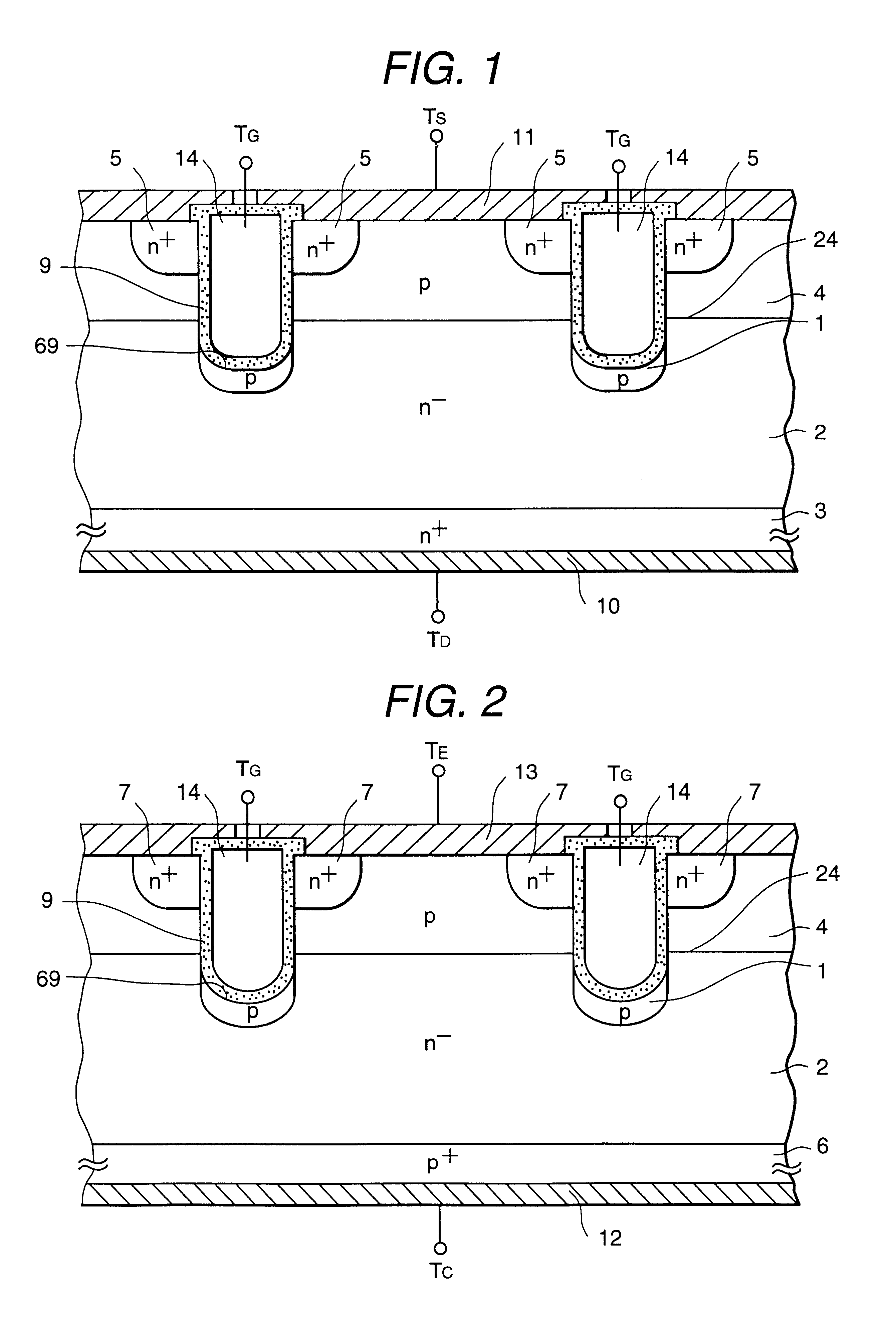
FIG. 1 shows a cross-sectional view of the unit segment of n channel SiC(silicon carbide) MOSFET of withstand voltage 2500V class in the embodiment 1 of the present invention. In FIG. 1, TS is a source terminal, TD is a drain terminal, and TG is a gate terminal In this embodiment, the segment width is 5 .mu.m and its depth is 1 mm. Other structural specifications are defined as below. The n- conduction type drift layer 2 is formed on the n+ conduction type drain layer 3 and its thickness is approximately 20 .mu.m. The thickness of the n+ conduction type drain layer 3 is about 300 .mu.m, the thickness of the p conduction type body layer 4 is 4 .mu.m, the junction depth of the p+ conduction type source region 5 and the p conduction type electric field relaxation semiconductor region 1 is individually 0.5 .mu.m, the depth of the concave portion, that is, trench 69 is 6 .mu.m, and the width of the trench is 3 .mu.m, the thickness of the insulator layer 9 such as SiO2 (silicon oxide) for...

embodiment 2

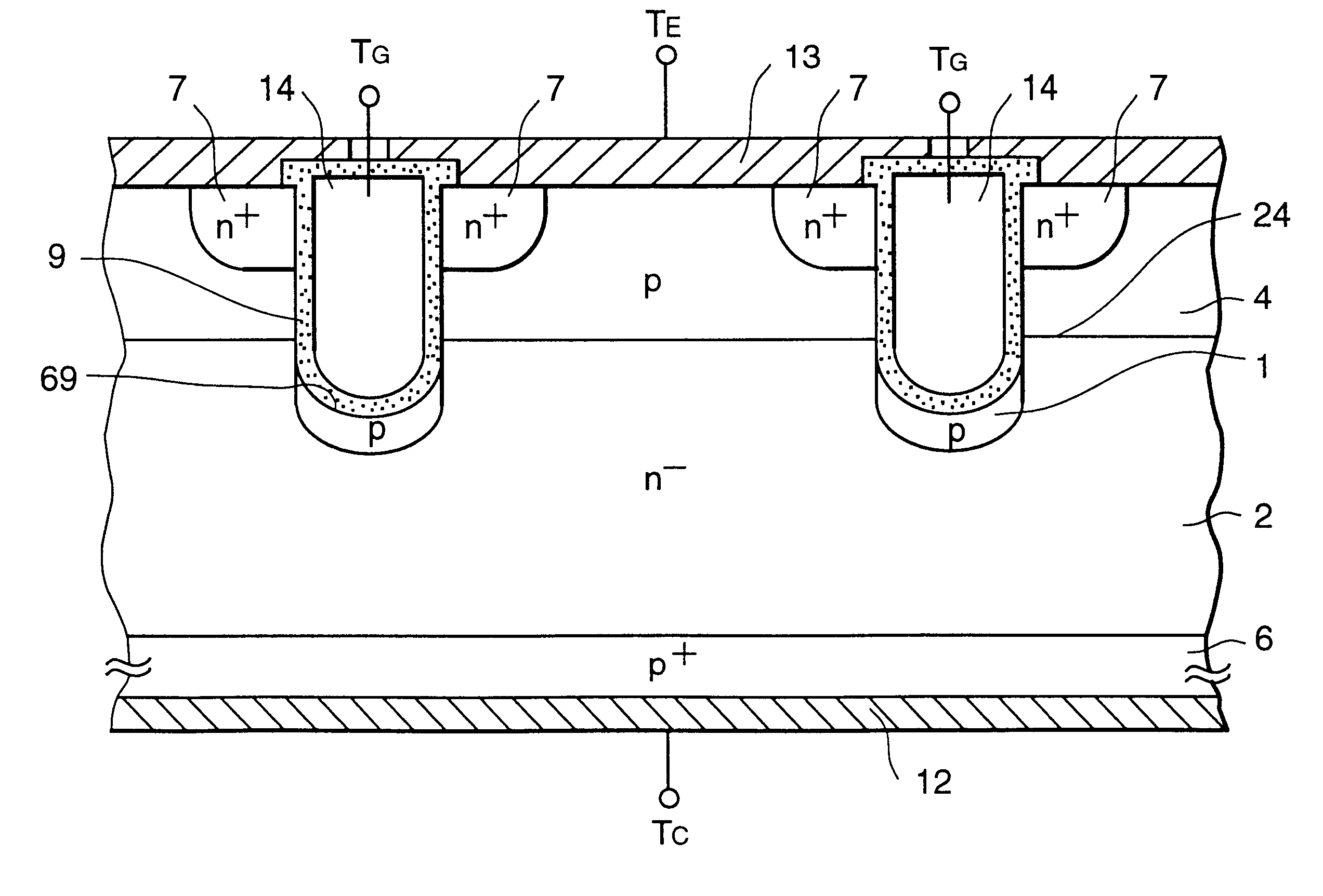
FIG. 2 is a cross-sectional view of the unit of n channel SiC IGBT in the embodiment 2 of the present invention. In FIG. 2, TE is an emitter terminal, and TC is a collector terminal. In the structure of the device in FIG. 2 the p conduction type collector layer 6 is formed instead of the n+ conduction type drain layer 3 in the embodiment 1. In the structural specifications and fabrication method in the embodiment 2, a difference from the embodiment 1 is only that a SiC p+ conduction type substrate is used instead of a SIC n+ conduction type substrate, but other aspects are similar to the embodiment 1. The impurity density of the p+ conduction type substrate is between 10.sup.18 atm / cm.sup.3 and 10.sup.19 atm / cm.sup.3.

In the operation of the n channel IGBT of this embodiment, at first, the gate voltage to be applied is so adjusted that the electric potential of the collector electrode 12 may be higher than the electric potential of the emitter electrode 11 and that the electric poten...

embodiment 3

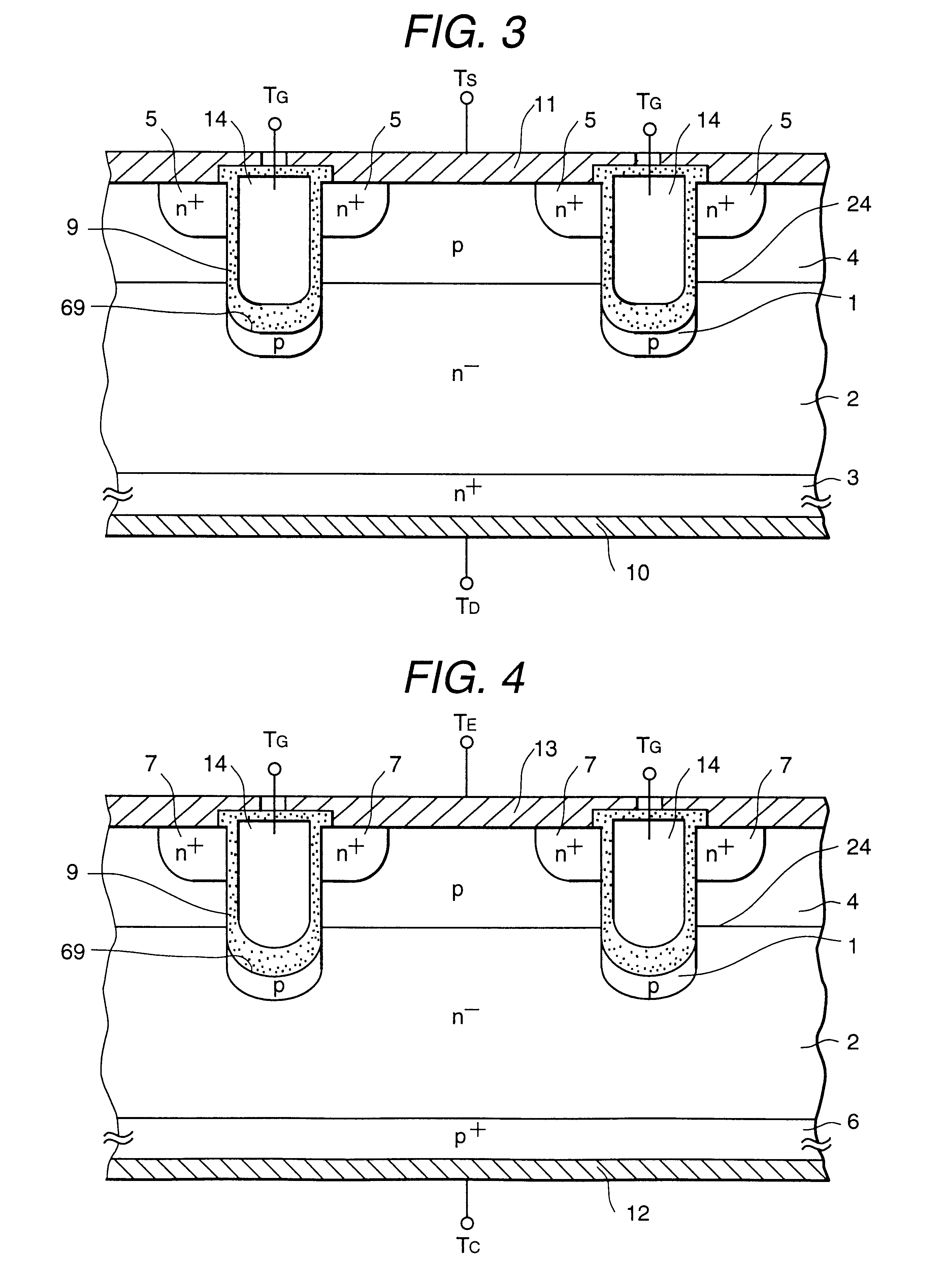
FIG. 3 shows a cross-sectional view of the unit segment of n channel SiC(silicon carbide) MOSFET of withstand voltage 2500V class in the embodiment 3 of the present invention. In this embodiment, the segment width is 5 .mu.m and its depth is 1 mm. Other structural specifications are defined as below. The n- conduction type drift layer 2 is formed on the n+ conduction type drain layer 3 and its thickness is approximately 20 .mu.m. The thickness of the n+ conduction type drain layer 3 is about 300 .mu.m, the thickness of the p conduction type body layer 4 is 4 .mu.m, the junction depth of the p+ conduction type source region 5 and the p conduction type electric field relaxation semiconductor region 1 is individually 0.5 .mu.m, the depth of the concave portion, that is, trench 69 is 6 .mu.m, and the width of the trench is 3 .mu.m, the thickness of the insulator layer 9 such as SiO2 (silicon oxide) formed in side the trench 96 is 0.5 .mu.m at the bottom portion and 0.1 .mu.m lateral por...


PUM


Abstract

In a semiconductor device having a trench type insulated gate structure, in the case where a drift layer 2 of an n- conduction type has a high carrier density, when a high voltage is applied between a drain and a source in such a manner that a channel is not formed, the electric field strength of an insulator layer 9 below the trench type insulated gate is increased, thus causing breakdown. The withstand voltage of the semiconductor device is limited by the breakdown of the insulator layer 9, and it is difficult to realize high withstand voltage.In the characteristic of the present invention, a field relaxation semiconductor region 1 of a conduction type opposite to the conduction type of the drift layer 2 is formed within the drift layer 2 below the insulator layer 9 in the trench of the trench type insulated gate semiconductor device. Also, the thickness of a bottom portion of the insulator layer 9 provided in the trench of the trench type insulated gate semiconductor device is made significantly greater than the thickness of a lateral portion thereof.

Description

The present invention relates to an insulated gate semiconductor device used as a switching device.Conventionally, MOSFET and Insulation Gate Type Bipolar Transistor (hereinafter referred to as IGBT ) are well known as vertical type power semiconductor devices which have advantages in high speed switching characteristics, high input impedance and low input loss. In order to reduce the resistance of the junction field effect transistor (hereinafter referred to as JFET) immanent in above individual semiconductor devices and establish low-loss, what are used for both transistors are semiconductor devices having a trench type insulated gate structure having a gate 14 in the concave portion 29 as shown in FIGS. 11 and 12.In such conventional semiconductor devices having a trench type insulated gate structure as shown in FIGS. 11 and 12, in case that the carrier density in the n- conduction type drift layer 2 as a semiconductor substrate having the first conduction type (n) is larger, the...

Claims


Application Information

Patent Timeline
Patent Type & Authority Patents(United States)
IPC IPC(8): H01L29/02H01L29/78H01L29/66H01L29/06H01L29/739H01L29/10H01L29/40H01L29/423H01L29/24
CPCH01L29/0619H01L29/1095H01L29/7813H01L29/7397H01L29/1608H01L29/7809H01L29/42368H01L29/7811
Inventor SUGAWARA, YOSHITAKAASANO, KATSUNORI
Owner HITACHI LTD
Why Eureka
Try Eureka