Thin-film transistor with lightly-doped drain

a thin film transistor and drain technology, applied in the direction of static indicating devices, identification means, instruments, etc., can solve the problems of significant deterioration phenomena, difficult to provide elements having sufficient performance, and more severe requirements on the operation performance (especially, operating speed) of tfts

Inactive Publication Date: 2002-03-19
SEMICON ENERGY LAB CO LTD
View PDF11 Cites 104 Cited by
  • Summary
  • Abstract
  • Description
  • Claims
  • Application Information

AI Technical Summary

Problems solved by technology

However, the accelerating trend toward AMLCDs with higher performance in recent years has resulted in more severe requirements on the operational performance (especially, operating speed) of TFTs.
It has therefore become difficult to provide elements having sufficient performance utilizing TFTs comprising amorphous silicon films because of their operating speed.
First, since an active layer as a whole employed in such structures is as very thin as about 50 nm, impact ionization occurs at

Method used


Image

  • Thin-film transistor with lightly-doped drain
  • Thin-film transistor with lightly-doped drain
  • Thin-film transistor with lightly-doped drain

Examples


first embodiment

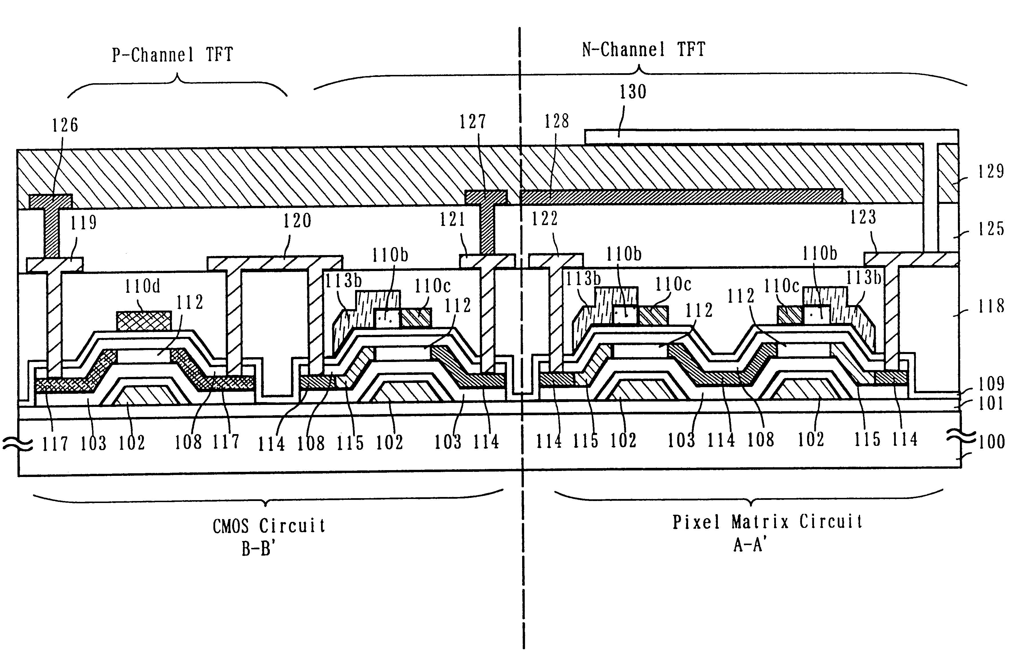
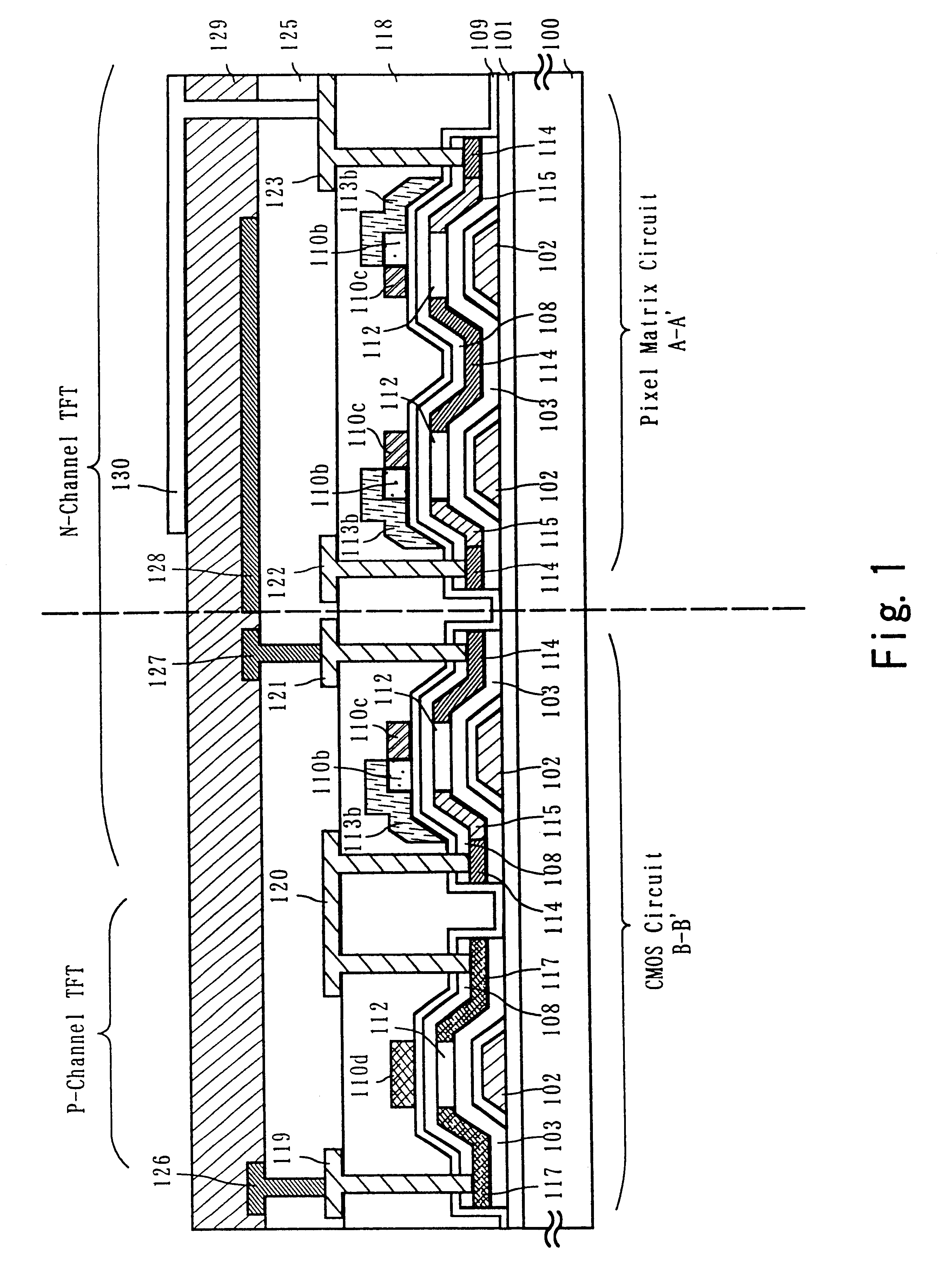
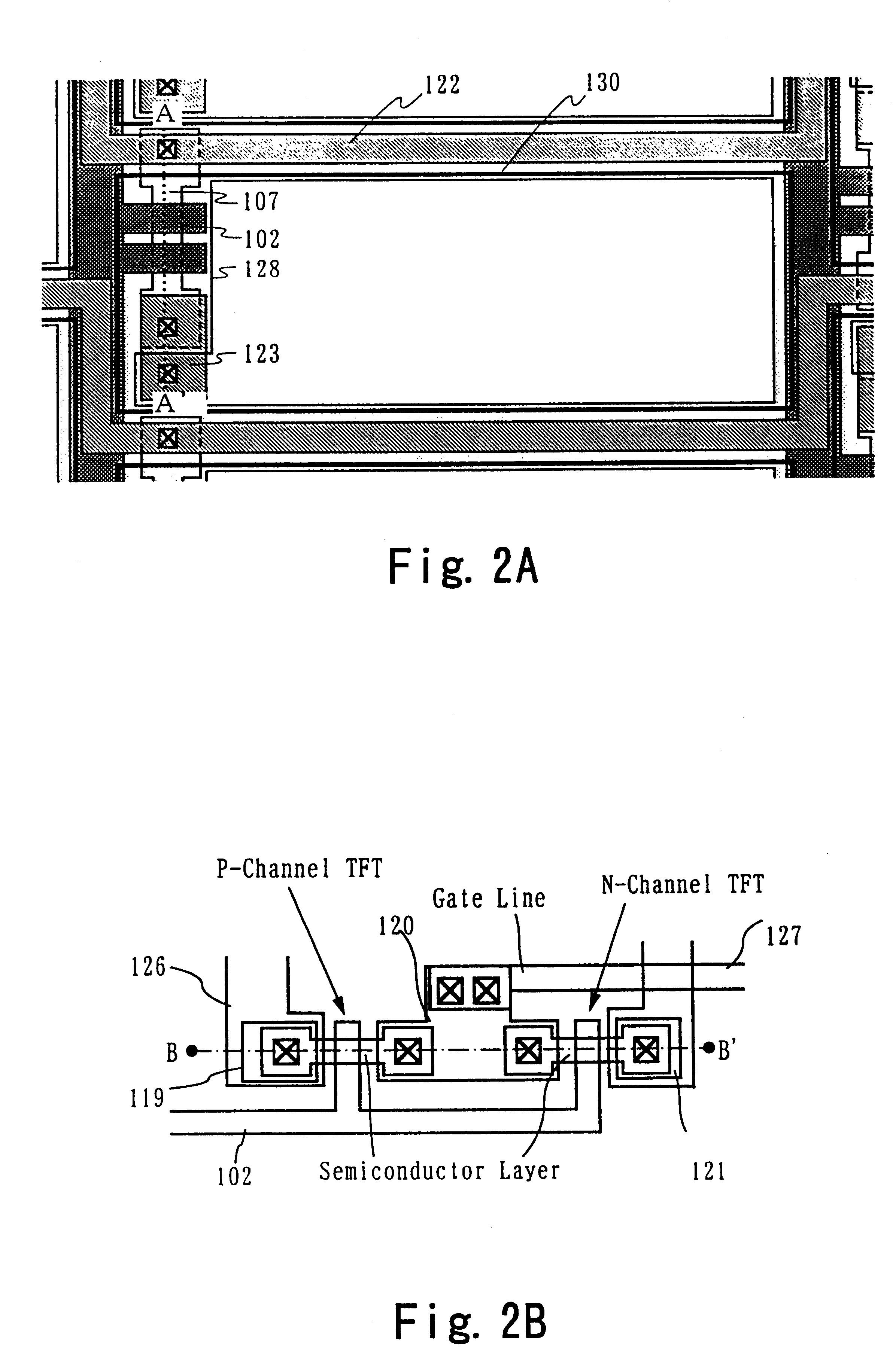
A first embodiment will now be described. A typical embodiment of the present invention will now be described with reference to FIGS. 1 through 4. The present embodiment will be described with reference to a CMOS circuit that forms a part of a peripheral driving circuit portion and a pixel TFT that forms a part of a pixel matrix circuit portion provided on the same substrate. A description will be made with reference to FIGS. 3 and 4 on a method for manufacturing a semiconductor device including a semiconductor circuit formed by semiconductor elements according to the invention.

A substrate 100 is first prepared. The substrate 100 may be a glass substrate, a quartz substrate, an insulating substrate such as crystalline glass, a ceramic substrate, a stainless steel substrate, a metal (tantalum, tungsten, molybdenum or the like) substrate, a semiconductor substrate, a plastic substrate (polyethylene terephtalate substrate) or the like. In the present embodiment, a glass substrate (Coni...

second embodiment

A second embodiment will now be described. The present embodiment is an example in which a crystalline semiconductor film is obtained using a method different from that in the first embodiment. In the present embodiment, a step is added between the steps shown in FIGS. 3B and 3C of the first embodiment to cause a catalytic element for promoting crystallization to be carried on the entire surface of the semiconductor film or to be selectively carried. Since the present embodiment is substantially the same as the first embodiment in the basic configuration, the following description will address only differences between them.

The present embodiment is identical to the first embodiment up to the step of forming the semiconductor film 104 (FIG. 3B).

According to the present embodiment, a catalytic element for promoting the crystallization of silicon is introduced on the surface of the semiconductor film 104. As the catalytic element for promoting the crystallization of silicon, one or a p...

third embodiment

the invention will now be described. The present invention is an example in which a crystalline semiconductor film is obtained using a method different from that for the first embodiment. In the present embodiment relates to a method wherein laser beams are shaped into a rectangular or square configuration to perform a uniform laser crystallization process throughout an area in the range from several cm.sup.2 to several hundred cm.sup.2 with irradiation at one time, thereby providing a crystalline silicon film. Since this embodiment is substantially the same as the first embodiment in its basic configuration, the description will address only differences between them.

According to the present embodiment, irradiation is conducted with excimer laser light which is processed into a planar configuration at the step shown in FIG. 3C. The laser light must be processed into a planar configuration such that an area on the order of several tens cm.sup.2 (preferably 10 cm.sup.2) or more can be...


PUM


Abstract

There is provided a semiconductor device including a semiconductor circuit formed by semiconductor elements having an LDD structure which has high reproducibility, improves the stability of TFTs and provides high productivity and a method for manufacturing the same.In order to achieve the object, the design of a second mask is appropriately determined in accordance with requirements associated with the circuit configuration to make it possible to form a desired LDD region on both sides or one side of the channel formation region of a TFT.

Description

1. Field of the InventionThe present invention relates to a structure of a semiconductor device having a semiconductor circuit comprised of semiconductor elements such as insulated gate transistors and a method for manufacturing the same. More particularly, the invention relates to a structure of a semiconductor device having a semiconductor circuit comprised of semiconductor elements having an LDD structure formed of organic resin and a method for manufacturing the same. Semiconductor devices according to the invention include not only elements such as thin film transistors (TFTs) and MOS transistors but also displays having a semiconductor circuit and electro-optical devices such as image sensors formed by such insulated gate transistors. In addition, semiconductor devices according to the invention include electronic equipments loaded with such displays and electro-optical devices.2. Description of the Related ArtTFTs have been conventionally used as switching elements of active ...

Claims


Application Information

Patent Timeline
IPC IPC(8): H01L21/02H01L21/336H01L29/66H01L21/84H01L21/70H01L27/12H01L29/786G09F9/33H01L21/77
CPCH01L27/1237H01L27/1296H01L29/66765H01L29/78684H01L29/78627H01L29/78678H01L29/78624
Inventor YAMAZAKI, SHUNPEINAKAJIMA, SETSUOKUWABARA, HIDEAKI
Owner SEMICON ENERGY LAB CO LTD
Why Eureka
Try Eureka