
Wafer transfer station for a chemical mechanical polisher

a technology of mechanical polishing and transfer station, which is applied in the direction of lapping machines, furnaces, charge manipulation, etc., can solve the problems of bottleneck in the movement of wafers into and out of the polisher

Inactive Publication Date: 2002-03-26
APPLIED MATERIALS INC
View PDF12 Cites 17 Cited by
  • Summary
  • Abstract
  • Description
  • Claims
  • Application Information

AI Technical Summary

Benefits of technology

This solution reduces wafer transfer time, minimizes the risk of damage and contamination, and increases throughput by allowing simultaneous handling of multiple wafers, enhancing the efficiency of the CMP process.

Problems solved by technology

More specifically, the process of transferring the wafer into and out of a single load / unload pedestal with a transfer robot that can only transport one wafer at a time causes a bottleneck in wafer movement into and out of the polisher.

Method used


Image

  • Wafer transfer station for a chemical mechanical polisher
  • Wafer transfer station for a chemical mechanical polisher
  • Wafer transfer station for a chemical mechanical polisher

Examples


Embodiment Construction

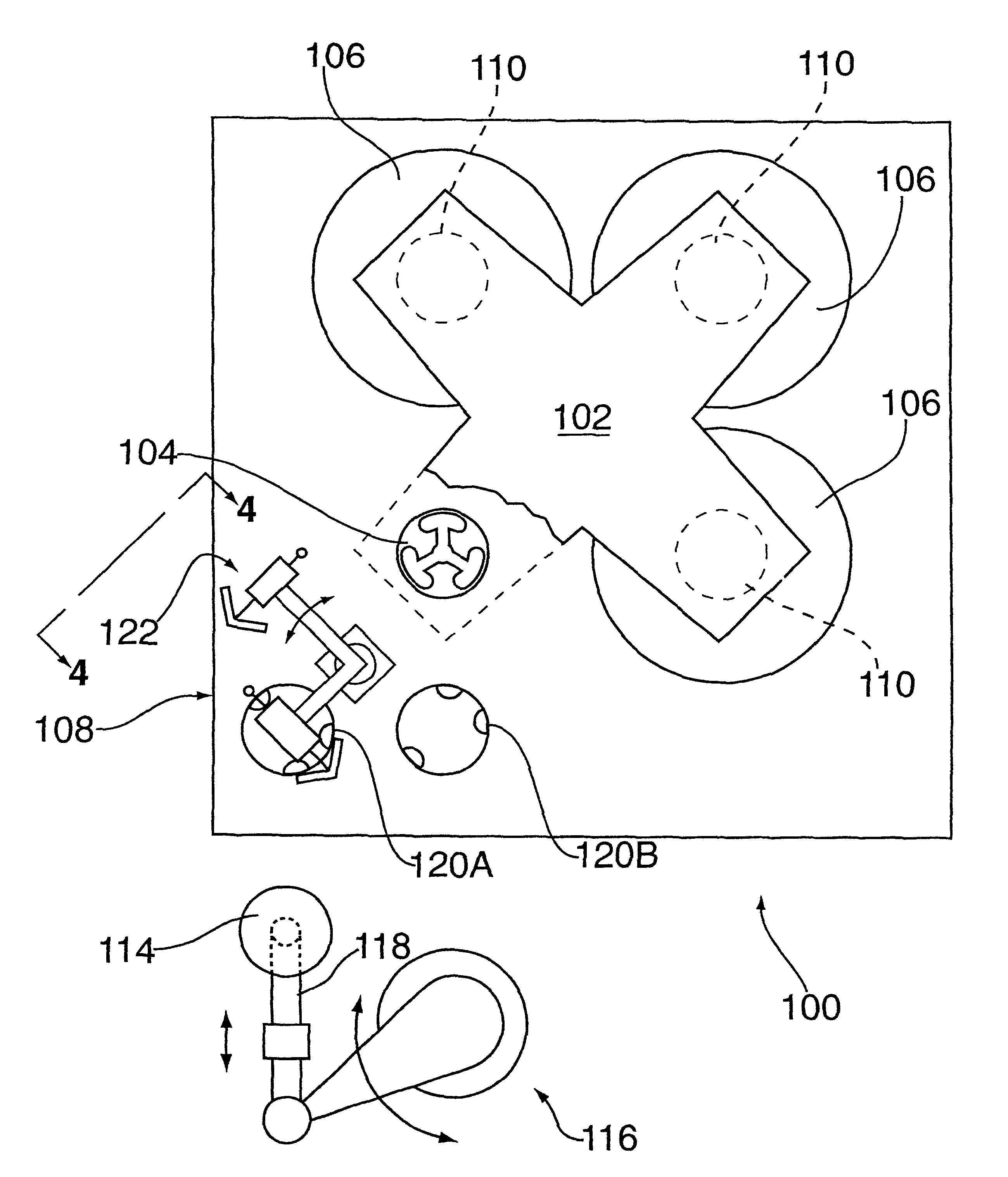
FIG. 1 depicts a schematic top plan view of a chemical mechanical polisher 100. The polisher 100 has a plurality of polishing stations 106 (e.g., three), a carousel 102 that supports four polishing heads 110, a wafer load / unload assembly 104, and a transfer station 108. An input / output robot 116 loads and unloads wafers 114 to / from the transfer station 108. Four polishing heads 110 are mounted in the carousel 102. The carousel 102 is partially cut-away to provide a view of the components of the transfer station 108. As such, one of the four polishing heads 110 is not shown. The carousel 102 rotates about a central axis such that any one of the polishing heads 110 may be positioned at any one of the polishing stations 106 or the transfer station 108. Consequently, the wafer 114 can be loaded into a particular polishing head 110, and the carousel 102 can move the head 110 to a particular polishing station 106.

The wafer 114 is transferred between the polisher 100 and other systems (e.g...


PUM

PropertyMeasurementUnit
diameteraaaaaaaaaa
diameteraaaaaaaaaa
diameteraaaaaaaaaa

Abstract

A transfer station and concomitant method for a chemical mechanical polishing system comprising a pair of buffer stations and a transport robot. The buffer stations and the ability to transport two wafers simultaneously with the transfer robot minimizes the exchange time for loading and unloading wafers into the chemical mechanical polishing system. The lowering of the exchange time improves the number of wafers processed per hour by the chemical mechanical polishing system. The transfer robot utilizes wafer edge grip features, adjustable wafer gripper force, minimum wafer contact points, fluid media for wafer present sensing, and mechanical interlocking mechanisms to protect both the wafer and the transfer station.

Description

BACKGROUND OF THE DISCLOSURE1. Field of InventionThe present invention relates generally to a chemical mechanical polishing system. More specifically, the invention relates a method and apparatus for positioning a workpiece or semiconductor wafer into a chemical mechanical polishing system.2. Background of Prior ArtIn semiconductor wafer processing, the use of chemical mechanical polishing, or CMP, has gained favor due to the enhanced ability to stack multiple feature layers on a semiconductor workpiece, or wafer. As the demand for polishing wafers as part of a semiconductor fabrication process increases the requirement for higher processing rates while minimizing risk of wafer damage and contamination has correspondingly experienced greater urgency for improvement.Two such CMP systems that address these issues are described in a commonly assigned patent to Perlov et al. (U.S. Pat. No. 5,804,507, issued Sep. 8, 1998) and in a commonly assigned patent to Tolles et al. (U.S. Pat. No. ...

Claims


Application Information

Patent Timeline
Patent Type & Authority Patents(United States)
IPC IPC(8): B24B37/04B24B41/00H01L21/67H01L21/677B24B37/34B25J15/00B25J15/08B65G49/07H01L21/304
CPCB24B37/345H01L21/67745B24B41/005Y10S414/135H01L21/304
Inventor TOBIN, JIM
Owner APPLIED MATERIALS INC
Learn More