

Method and apparatus of correcting design-patterned data, method of electron beam and optical exposure, method of fabricating semiconductor and photomask devices
- Summary
- Abstract
- Description
- Claims
- Application Information
AI Technical Summary
Benefits of technology
Problems solved by technology
Method used
Image

Examples
example 2
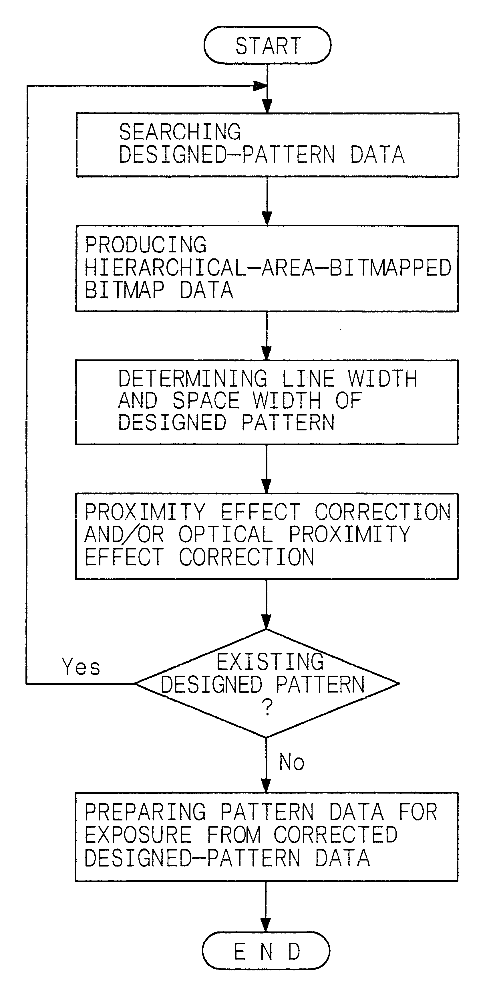
Example 2 is concerned with the method of electron beam exposure, the photomask and the method of fabrication of the photomask, provided by the present invention. That is, concerning the method of electron beam exposure, for example, designed-pattern data obtained by data-processing a plurality of designed patterns for the fabrication of a semiconductor device are corrected, and an electron beam resist formed on a substrate is exposed with an electron beam on the basis of pattern data for electron beam exposure produced from the corrected designed-pattern data. The substrate used in Example 2 is a mask blank. Concerning the photomask and the method of fabrication of the photomask, then, an etching mask obtained by developing the electron beam resist is used for etching a mask blank. Designed-pattern data is corrected according to the method of correcting designed-pattern data, provided by the present invention, including the hierarchical-area-bitmapping procedure explained in Exampl...
example 3
Example 3 is also concerned with the method of electron beam exposure, more specifically, with the method of electron beam exposure in which an electron beam resist formed on a substrate is directly exposed with an electron beam. In Example 3, the substrate is constituted of a metal layer 22 of an aluminum alloy formed above a semiconductor substrate 20 as shown in a schematic partial cross-sectional view in FIG. 6A, while the substrate shall not be limited to the above structure. Numeral 21 indicates an insulation interlayer formed on the semiconductor substrate 20. Concerning the method of electron beam exposure in Example 3, designed-pattern data obtained by data-processing a plurality of designed patterns, e.g., for the fabrication of a semiconductor device are corrected, and an electron beam resist 23 formed on the metal layer 22 as a substrate is exposed with an electron beam on the basis of the pattern data for electron beam exposure prepared on the basis of the corrected des...
example 4
Example 4 is concerned with the method of optical exposure, the semiconductor device and the method of fabrication of the semiconductor device, provided by the present invention. That is, concerning the method of optical exposure, for example, designed-pattern data obtained by data-processing a plurality of designed patterns is corrected, and an electron beam resist formed on a mask blank is exposed with an electron beam on the basis of the pattern data for electron beam exposure prepared from the corrected designed-pattern data. Then, the above electron beam resist is developed to obtain an etching mask, and the mask blank is etched with the etching mask to fabricate the photomask. The photomask provided by the present invention is used in the method of optical exposure. That is, a photo resist formed on a substrate is exposed with exposure light to transfer a pattern formed on the photomask to the photo resist formed on the substrate. Concerning the semiconductor device and the me...
PUM
 Abstract
Description
Claims
Application Information